Multilayer PCB
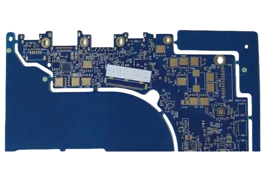
Multilayer PCB sample display produced by HXPCB
HXPCB focuses on the research and development of ultra-large size circuits board, multi-layer PCBs, metal-based PCBs, rigid-flex high-frequency PCBs, HDI PCBs, and related processes. We offer comprehensive services, including PCB design, prototyping, processing, and assembly.

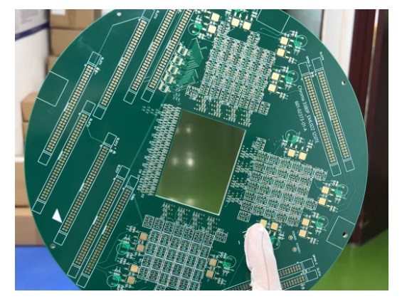
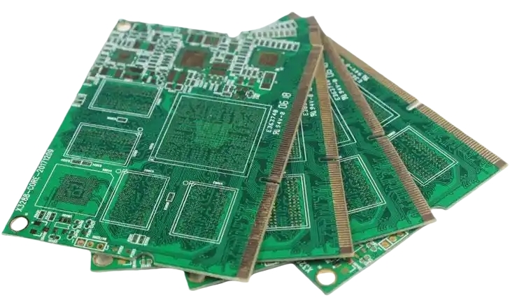

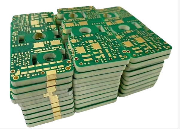
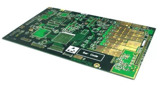


Advantages of HXPCB in Multilayer Boards
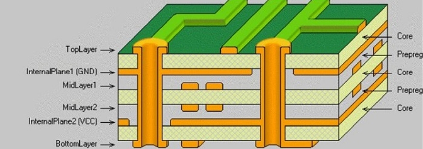
A multi-layer PCB is a circuit board with multiple conductive layers, usually made up of alternating insulating layers and conductor layers. Compared with single-layer PCBs (only one conductive layer) and double-layer PCBs, multi-layer PCBs can provide higher circuit density and complexity in a relatively small volume. Multi-layer PCBs are generally composed of three or more layers, and the layers are connected by conductive through-holes. Different circuits can be arranged on each layer to meet the needs of complex electronic products.
What is a multilayer PCB?
A multi-layer PCB is a circuit board with multiple conductive layers, usually made up of alternating insulating layers and conductor layers. Compared with single-layer PCBs (only one conductive layer) and double-layer PCBs, multi-layer PCBs can provide higher circuit density and complexity in a relatively small volume. Multi-layer PCBs are generally composed of three or more layers, and the layers are connected by conductive through-holes. Different circuits can be arranged on each layer to meet the needs of complex electronic products.
Characteristics of multilayer PCB
1. High circuit density
Multilayer PCB can achieve higher circuit density and is suitable for equipment with complex functions and high integration, such as high-performance computers, communication equipment, etc.
Support wiring technology with fine line width/spacing (such as less than 2 mil).
2. Excellent electrical performance
Power and ground layering: Multilayer PCB can design dedicated power layer and ground layer to provide a stable electrical reference plane.
Signal integrity: Support high-speed signal transmission and improve signal quality by optimizing wiring, reducing parasitic effects, and reducing signal reflections.
Low noise and low electromagnetic interference (EMI): Dedicated ground layer and shielding layer reduce the impact of EMI.
3. Support high-frequency and high-speed applications
Suitable for high-frequency (>300 MHz) and microwave (>3 GHz) applications, commonly used in communication equipment (such as 5G base stations, radar systems).
Special materials (such as PTFE, Rogers) are required to ensure low signal loss and low dielectric constant.
4. Complex manufacturing process
Involves complex inner layer lamination and interlayer alignment technology.
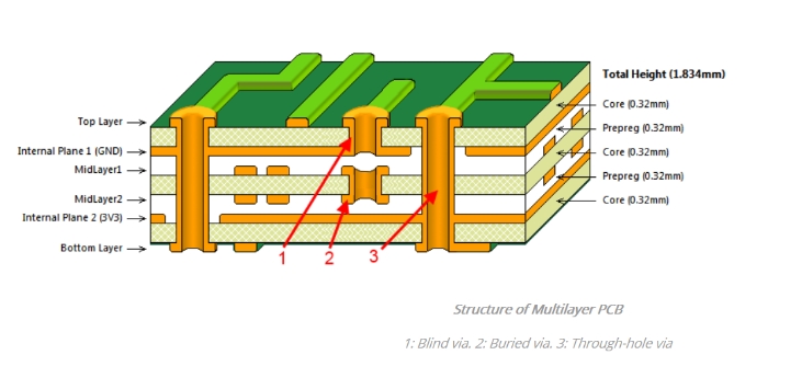
Multiple stacking and drilling: Including blind hole, buried hole and through hole design.
The inter-layer alignment accuracy and conductivity stability are extremely high.
5. Enhanced mechanical properties
The multi-layer PCB stacking structure enhances the mechanical strength of the board, and has stronger bending and impact resistance.
Supports larger PCB boards while maintaining flatness.
Technical difficulties in manufacturing multi-layer PCBs
1. The accuracy of the inner conductive lines is extremely high, especially in high-layer PCBs, where the line width and spacing usually need to reach the micron level.
2. Lamination requires precise alignment of multiple inner conductive lines with insulating layers while maintaining uniform compaction of the material.
3. Problems such as blistering, delamination or poor alignment are prone to occur during the lamination process.
4. The metallization of through holes or buried holes/blind holes in high-level PCBs requires uniform hole walls and no breaks.
5. Copper plating of through-holes with high aspect ratio is prone to uneven hole wall thickness. Multi-layer PCB requires strict control of impedance matching to reduce signal crosstalk and electromagnetic interference (EMI).
6. The dielectric constant (Dk) and loss factor (Df) of the material directly affect the signal transmission performance.
7. The alignment difficulty of each layer of high-level digital boards increases significantly, and slight deviations may lead to short circuits or open circuits.
8. The stacking of high-level PCBs can easily lead to heat accumulation, especially in high-power or high-frequency applications. Long-term use may cause thermal fatigue and mechanical stress.
9. Must be uniform across multiple layers to avoid impedance mismatch.
10. Processes such as immersion gold and OSP need to be evenly distributed in high-level digital boards.
11. Defect detection of high-level digital boards requires more advanced electrical testing technology (such as flying probe testing and ICT).
Multilayer PCB production process
1. Design data preparation
1.1 Data reception and review:
Check the Gerber files, material requirements, number of layers and design specifications provided by the customer.
Ensure that there are no DRC (design rule check) problems in the design, such as too small spacing or incorrect impedance control.
1.2 Stackup design:
Determine the board type (FR-4, high-frequency material, etc.), copper thickness, insulation layer thickness, etc. according to functional requirements.
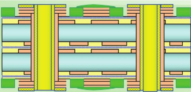
Generate a stackup diagram to ensure impedance matching and interlayer signal integrity.
2. Inner layer circuit production
2.1 Cleaning the copper clad board:
Cleaning the inner layer substrate by chemical and mechanical methods to remove the oxide layer.
2.2 Dry film coating:
Use a coating machine to apply photosensitive dry film to the inner copper surface.
Control the dry film thickness to ensure etching accuracy.
2.3 Exposure and development:
Use the exposure machine to transfer the circuit pattern using the photolithography film, and develop to remove the unexposed area.
2.4 Etching process:
Precisely etch the excess copper foil in the inner layer, leaving only the conductive circuit.
Control etching width and etching factor to avoid over-etching or under-etching.
2.5 Film removal and inspection:
Remove dry film and use automatic optical inspection (AOI) to check circuit integrity.
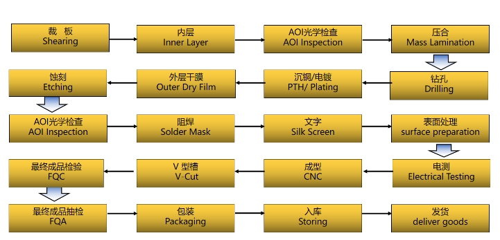
3. Inner layer lamination
3.1 Alignment and stacking:
Stack the processed inner layer with prepreg and outer copper foil according to the stacking diagram.
The optical alignment system ensures precise alignment between inner layers.
3.2 Lamination process:
Use a laminator to apply high temperature (170200℃) and high pressure (150200psi) to the board.
Control the heating curve and holding time to allow the prepreg to flow and solidify fully.
Prevent interlayer gaps or delamination problems to ensure lamination quality.
4. Drilling
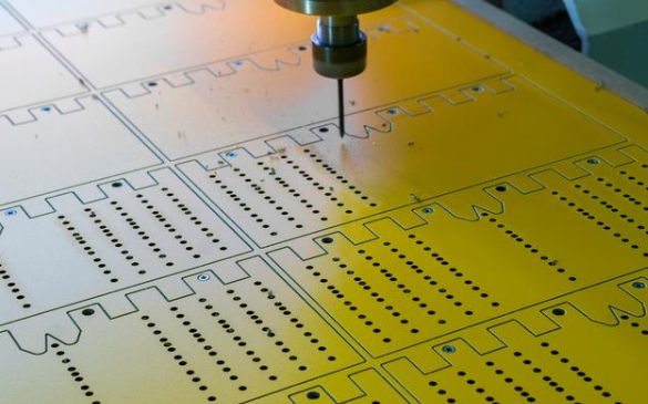
4.1 CNC drilling:
The CNC drilling machine completes through-hole, blind hole or buried hole processing.
For high-layer boards, attention should be paid to the porous structure and deep and wide resin residues to prepare for subsequent hole metallization.
Ensure the cleanliness and roughness of the hole wall, and the ratio should be controlled within a reasonable range (such as within 10:1).
4.2 Hole wall treatment:
Use plasma or chemical methods to remove the hole wall to improve copper adhesion.
5. Hole metallization
5.1 Chemical copper deposition:
Form a uniform initial copper layer (thickness 1-2μm) on the hole wall.
Control the reaction speed and uniformity of chemical deposition to avoid copper fracture on the hole wall.
5.2 Electroplating thickening:
The electroplating process further thickens the hole wall copper layer (usually up to 20~25μm), enhancing mechanical strength and conductivity.
Pulse electroplating technology improves the uniformity of the plating.
Application of multi-layer PCB
| Consumer Electronics | Smartphones, TVs, tablets, and wearables |
| Communication Devices | Smartphones, laptops, tablets, and routers |
| High-Performance Computing (HPC) | Supercomputers, data centers, and cloud servers |
| Medical Equipment | MRI machines, ultrasound devices, and pacemakers |
| Automotive Electronics | Infotainment systems, ADAS, and electric control units |
| Aerospace and Defense | Radar systems, navigation systems, and drones |
| Energy and Power | Solar panels, wind turbines, and energy storage systems |
| Military Electronics | Surveillance systems, communication gear, and weapon systems |
| LED Lighting | LED bulbs, panels, and street lighting |
Common parameters of multi-layer PCB
| Parameter | Multilayer PCB | Regular PCB |
| Substrate Material | High-performance materials: Rogers, PTFE, Teflon, High-Tg FR-4 | Standard FR-4 |
| Dielectric Constant (Dk) | 2.2–4.5 (low and stable for high frequencies) | 4.2–4.8 (suitable for general use) |
| Loss Tangent (Df) | ≤0.002 (low loss for RF and high-speed signals) | 0.015–0.020 |
| Glass Transition Temperature (Tg) | Typically 170–260°C (High-Tg materials) | 130–150°C |
| Thermal Conductivity | 0.25–1.0 W/m·K (better heat dissipation) | 0.25–0.4 W/m·K |
| CTE (Coefficient of Thermal Expansion) | Low (e.g., 20 ppm/°C) for high reliability | Higher (e.g., 50 ppm/°C), suitable for general designs |
| Material Stability | Excellent at high frequencies and temperatures | Moderate, adequate for basic applications |
| Surface Finish Options | ENIG, Immersion Silver, Immersion Tin, OSP | HASL, OSP |
| Moisture Absorption | <0.1% (critical for RF and microwave) | ~0.2% |
| Flame Retardancy | V-0 (high reliability) | V-0 |
| Parameter | Multilayer PCB | Regular PCB |
| Number of Layers | 4–64 layers or more | 1–2 layers |
| Board Thickness | 0.4–3.2 mm | 0.6–2.0 mm |
| Copper Thickness | 0.5 oz–3 oz per layer | 1 oz–2 oz |
| Minimum Trace Width/Spacing | 2–4 mil | 6–8 mil |
| Minimum Drill Hole Size | 0.1 mm (mechanical), 0.075 mm (laser) | 0.2 mm (mechanical) |
| Aspect Ratio | Up to 12:1 | 8:1 |
| Material Type | High-performance materials (e.g., Rogers, PTFE, FR-4) | Standard FR-4 |
| Dielectric Constant (Dk) | 2.2–4.5 | 4.2–4.8 |
| Loss Tangent (Df) | ≤0.002 | 0.015–0.020 |
| Impedance Control | Precise (±5% tolerance) | Typically absent |
| Thermal Conductivity | 0.25–1.0 W/m·K | 0.25–0.4 W/m·K |
| Surface Finish | ENIG, Immersion Silver, OSP, HASL | HASL, OSP |
| Applications | High-frequency, high-speed circuits like 5G, radar, AI | Consumer electronics, basic control systems |
| Manufacturing Cost | High due to complexity | Low due to simpler design and manufacturing |
| Typical Challenges | Complex stack-up, impedance matching, reliability testing | Basic prototyping and simpler requirements |
| Parameter | Multilayer PCB | Regular PCB |
| Substrate Material | High-performance materials: Rogers, PTFE, Teflon, High-Tg FR-4 | Standard FR-4 |
| Dielectric Constant (Dk) | 2.2–4.5 (low and stable for high frequencies) | 4.2–4.8 (suitable for general use) |
| Loss Tangent (Df) | ≤0.002 (low loss for RF and high-speed signals) | 0.015–0.020 |
| Glass Transition Temperature (Tg) | Typically 170–260°C (High-Tg materials) | 130–150°C |
| Thermal Conductivity | 0.25–1.0 W/m·K (better heat dissipation) | 0.25–0.4 W/m·K |
| CTE (Coefficient of Thermal Expansion) | Low (e.g., 20 ppm/°C) for high reliability | Higher (e.g., 50 ppm/°C), suitable for general designs |
| Material Stability | Excellent at high frequencies and temperatures | Moderate, adequate for basic applications |
| Surface Finish Options | ENIG, Immersion Silver, Immersion Tin, OSP | HASL, OSP |
| Moisture Absorption | <0.1% (critical for RF and microwave) | ~0.2% |
| Flame Retardancy | V-0 (high reliability) | V-0 |
HXPCB provides multi-layer PCB assembly services
With more than ten years of experience and technology accumulation, HXPCB has become a trusted partner for customers. We provide multi-layer PCB assembly services from prototype design to mass production, covering high-complexity circuit boards with 4 to 64 layers. Whether it is high-frequency communication, data center, high-performance computing (HPC) or AI system, our professional team can easily solve it.
Choosing HXPCB is not only choosing advanced manufacturing technology, but also choosing a professional team to escort you throughout the process. We are committed to providing customers with efficient, reliable and customized multi-layer PCB assembly solutions.
FAQ
Frequently Asked Question
As layer count increases, the potential for improved signal integrity exists due to the ability to create dedicated ground and power planes, which can reduce noise and electromagnetic interference (EMI). However, improper layer stacking and routing can lead to issues such as crosstalk and increased inductance, which can degrade signal quality.
For high-frequency applications, materials like Rogers, PTFE, and High-Tg FR-4 are preferred due to their low dielectric constants and low loss tangents. These materials provide better performance in terms of signal integrity and thermal stability, essential for RF and microwave circuits.
The surface finish can significantly impact solderability, corrosion resistance, and the overall reliability of the PCB. For high-frequency applications, finishes like ENIG (Electroless Nickel Immersion Gold) and Immersion Silver are preferred due to their excellent electrical performance and reduced oxidation.
Impedance control is critical for high-speed and RF designs to ensure signal integrity. It involves matching the characteristic impedance of traces to the impedance of the connected components, which minimizes reflections and signal loss. This is achieved through careful trace width, spacing, and dielectric material selection.
The aspect ratio is calculated by dividing the PCB thickness by the diameter of the via. For example, if a PCB is 1.6 mm thick and the via diameter is 0.3 mm, the aspect ratio is 5.33:1. Higher aspect ratios can complicate the plating process and may require special considerations during manufacturing.
Thermal management is crucial in multilayer PCB design, especially for high-power applications. Effective thermal management strategies include using thermal vias, heat sinks, and appropriate material selection to dissipate heat efficiently and prevent thermal damage to components.
Reliable connections in multilayer PCBs are ensured through proper via plating, adequate solder joint design, and the use of appropriate surface finishes. Additionally, thermal and mechanical stresses should be considered to prevent delamination and ensure long-term reliability.
Improving yield in multilayer PCB production can be achieved through rigorous design reviews, implementing automated optical inspection (AOI) systems, and optimizing manufacturing processes. Regular maintenance of equipment and training for staff also contribute to higher yield rates.