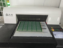
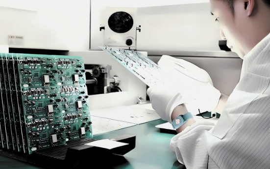
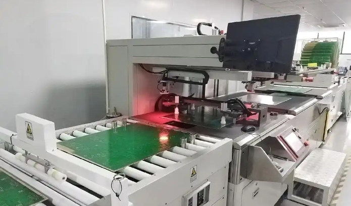
multi-layer PCB
High-end design,
Read MoreHXPCB focuses on the research and development of ultra-large size circuits board, multi-layer PCBs, metal-based PCBs, rigid-flex high-frequency PCBs, HDI PCBs, and related processes. We offer comprehensive services, including PCB design, prototyping, processing, and assembly.
PCB box assembly refers to the additional assembly work carried out around the completed PCB assembly (PCBA), including the assembly and connection of the PCB into the housing and related components. It focuses on the installation of PCB and its related functional modules, usually at the semi-finished product level.
1. Finished PCBs
The fully assembled and tested PCBs are installed in an enclosure or housing.
2. Cable and Harness Installation
The routing and installation of connectors, wires, and cable assemblies to ensure proper communication between the PCBs and other components.
3. Subcomponent Assembly
Additional subcomponents such as displays, switches, sensors, or power supplies are added to enhance the functionality of the system.
4. Enclosure Assembly
The enclosure is made of plastic, metal, or other materials and is installed around the PCBs and other components to provide structural integrity and protection.
Design review: DFM analysis, optimization of PCB layout and shell matching.
Material procurement: BOM list confirmation, key component channel review (avoid counterfeit).
PCB assembly: dual-track SMT patch + selective wave soldering (complex mixed technology board).
System integration: wiring harness assembly, heat sink installation, display/button integration.
Testing and packaging: aging test, IP protection level test (such as IP67), customized packaging solution.
HXPCB has more than 10 years of experience in PCB manufacturing and assembly, focusing on the assembly and manufacturing of high-frequency, high-density and complex multi-layer PCBs.
HXPCB provides complete PCB Box Build Assembly services, covering every link of the product from components to finished products
HXPCB focuses on customer needs and provides highly customized services to meet different project requirements from prototype development to mass production.
HXPCB adopts advanced quality management systems in every link, and has passed ISO9001, UL and RoHS certifications to ensure that products meet international standards.
HXPCB has advanced production facilities and efficient supply chain management, quickly responds to customer needs, and achieves fast product delivery.
HXPCB has an experienced engineering team to provide customers with full technical support, assist in optimizing design, and improve production efficiency.

Anti-vibration/high and low temperature design, EMC shielding optimization, suitable for harsh factory environments.

Biocompatible housing materials, aseptic workshop assembly, compliant with FDA/IEC 60601 standards.

Ultra-thin design, diversified surface treatment (anodizing, silk screen, laser engraving).
Cost control: Large-scale procurement reduces BOM costs and supports localized alternatives
Fast delivery: Standard products are delivered in 15 days, and expedited services are delivered in 7 days (30% faster than the industry average).
Flexible orders: Small batch orders of 1-1000 units are available, suitable for product verification of start-ups.
Global compliance: Provide full support for target market certification (including document preparation and laboratory docking).
Through-hole PCB assembly provides higher mechanical strength and durability, is suitable for high-power, high-current applications, and is convenient for later maintenance.
Through-hole PCB assembly usually requires materials such as PCB board, components, solder, soldering tools and cleaners. The choice of materials depends on the design requirements of the circuit board.
The lead time depends on the size and complexity of the order. Typically, small-volume orders have shorter lead times, while large-volume orders take longer.
We ensure the assembly quality meets the standards through a strict quality control process including automatic optical inspection (AOI), X-ray inspection and functional testing.
Through-hole technology solders components by inserting component pins into holes, while surface mount technology (SMT) solders components directly to the PCB surface. Through-hole is suitable for applications that require stronger physical connections, while SMT is more suitable for high-density, high-speed assembly.
Yes, many PCBs can use both through-hole and surface mount technology, called hybrid assembly. This allows the advantages of both technologies to be used to meet different design needs.
Yes, we provide customized through-hole PCB assembly services, designing and optimizing the assembly process according to the specific needs of customers.
The cost of through-hole PCB assembly depends on several factors, including the number of PCB boards, component types, assembly complexity, and production batch.