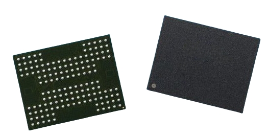
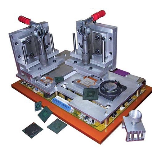
BGA Assembly
Selected PCB samples BGA assembly display
HXPCB focuses on the research and development of ultra-large size circuits board, multi-layer PCBs, metal-based PCBs, rigid-flex high-frequency PCBs, HDI PCBs, and related processes. We offer comprehensive services, including PCB design, prototyping, processing, and assembly.


What is BGA assembly
BGA (Ball Grid Array) is a common semiconductor packaging technology used to connect integrated circuit (IC) chips to circuit boards. The BGA package is characterized by multiple solder balls (usually solder material) on the bottom surface, which form a grid-like arrangement, which can provide better electrical connection and heat dissipation performance.

The BGA package is connected to the PCB by placing an array of solder balls (usually solder) on the bottom of the chip. These solder balls are quickly electrically connected to the metal contact points (pads) on the PCB through a heated ignition device,However, BGA assembly (Ball Grid Array Assembly) is a surface mount technology (SMT) used to solder BGA packaged integrated circuits (ICs) onto printed circuit boards (PCBs).
BGA assembly process
The BGA assembly process usually includes the following steps:
Apply solder paste: Apply a layer of solder paste evenly on the pad of the PCB. This step is the key to subsequent soldering. The solder paste is usually applied by stencil printing technology or spraying technology to ensure the uniform application of the solder paste.
Place solder balls on pads: Use automated equipment (such as a placement machine) to accurately place the solder balls of the BGA chip on the PCB pads that have been soldered with solder paste. Subsequently, the solder balls of the BGA chip come into contact with the solder paste.
Reflow soldering: After the PCB and BGA components are placed, the entire PCB will enter the reflow soldering furnace for heating. By heating the solder paste to the melting point, the BGA solder balls and the PCB pads form an initialized solder connection.
Cooling and curing: After the reflow soldering is cooled, the PCB will slowly cool in the cooling area to solidify the solder joints.
Inspection and testing: After the matching is completed, automatic inspection (AOI), X-ray detection and other technologies are used to check the BGA soldering quality to ensure that there are no problems such as cold soldering, leaking soldering, open circuits or short circuits.
Advantages of HXPCB for BGA assembly
Efficient Space Utilization
Our BGA technology allows us to select the optimal pcb layout, thus optimizing the PCB design of compact devices. Making it ideal for applications where space is critical.
Better Heat Dissipation and Conductivity
Our BGA provides excellent heat dissipation and conductivity, reducing thermal stress and signal loss.
Higher Manufacturing Efficiency
Advanced assembly processes combined with sophisticated equipment ensure higher yields, reduce rework and improve overall manufacturing efficiency.
Reduced Wire Stress
The robust design of the BGA package minimizes mechanical stress on PCB traces and wires during operation, thereby increasing the durability and life of the component.
Reduced Costs
Our BGA assembly process reduces labor costs, and our technical support and staffing can reduce assembly time, reducing the operating and maintenance expenses of the final product.
Quality Assurance
HXPCB implements strict quality control measures, including X-ray and AOI inspections, to ensure defect-free assembly.
HXPCB's BGA assembly capabilities
| Category | Details |
|---|---|
| Supported BGA Types | Plastic BGA (PBGA), Ceramic BGA (CBGA), Ultra-Thin BGA (UTBGA), Chip-On-Package (CoP), Stacked Die BGA (SDBGA), Wafer-Level BGA (WLBGA), Fine-Pitch BGA (FPBGA), Quad Flat No-Lead (QFN) Packages |
| Assembly Size Range | Minimum: 3mm x 3mm / 2mm x 2mm; Maximum: 40mm x 40mm / 45mm x 45mm |
| Pitch Tolerance | Minimum pitch size: 0.35mm; Placement accuracy: +/- 0.025mm |
| Layer Support | Capable of assembling PCBs with up to 40 layers |
| Passive Component Sizes | Compatible with 01005, 0201, 0402, 0505, Press-fit components, Package-on-Package (POP) |
| Advanced Equipment | High-speed pick-and-place machines, precision solder jet printers, multi-zone reflow ovens, inline X-ray systems, and high-definition AOI systems |
| Service Types | Embedded Die BGA, High-Density BGA, Multi-Chip Module (MCM) Assembly, Organic Substrate BGA (OSBGA), and Hybrid Material BGA Assembly |
| Testing Capabilities | Functional testing, Boundary-scan testing, Real-time X-ray imaging, BGA Rework and Repair services, AOI and Solder Paste Inspection (SPI) |
Application of BGA assembly
| Autonomous Applications | Aerospace, Automotive |
| Test and Measurement Equipment | Semiconductors |
| Mobile Payments | Consumer Electronics |
| Industrial Electronics | RF Microwave |
| Wireless Devices | Military and Defense |
| Medical Devices | Wearable Electronics |