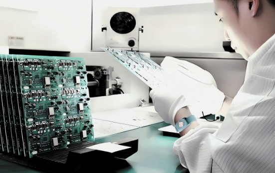
PCB (Printed Circuit Board) inspection is an important part of ensuring product quality, performance and reliability. The inspection steps usually involve multiple methods, covering all stages from production to assembly.
1. Visual Inspection
In the initial stage of PCB manufacturing, we generally perform manual or automatic visual inspection to detect the appearance defects of the board. This is the most basic inspection step, usually performed by an operator or using a machine vision system.
Inspection content:
Printing errors: whether there are unclear or incomplete circuit diagrams.
PCB surface: Check for damage, scratches or contaminants.
Alignment of pads and holes: Confirm whether the layout of pads and holes meets the design requirements.
Passive components and vias: Check for unsoldered components or via defects.
2. AOI inspection (Automated Optical Inspection)
AOI (Automated Optical Inspection) is a method of automatically detecting the accuracy of all components, circuits and solder joints on a PCB by using cameras and image processing algorithms. AOI can detect potential problems in real time during the production process.
Inspection content:
Solder joint inspection: Detect whether there are solder shorts, cold solder joints or solder balls.
Component location: Check whether the components are placed in the predetermined position, whether they are misplaced or installed in reverse.
Circuit integrity: Ensure that the PCB circuit is not broken or short-circuited.

3. Electrical Testing
Electrical testing is used to check the integrity and functionality of the PCB circuit to ensure that each electrical connection is normal.
Common electrical testing methods:
Flying Probe Testing: Testing through moving probes and contact points on the circuit board, suitable for small batch production.
ICT (In-Circuit Test): Directly check all electrical connections on the PCB through the test points to check electrical faults (such as open circuits, short circuits, wrong connections, etc.). Usually used for mass production.
Functional Test: Test whether the final function of the PCB meets the requirements. Commonly used for post-assembly testing to ensure the performance of the PCB in actual applications.
4. X-Ray Inspection
X-ray inspection is used to check the internal structure of the PCB, especially during the soldering process of high-density interconnect (HDI) or BGA (ball grid array) components. X-rays can be used to see the internal conditions of the solder joints to ensure the quality of soldering.
Inspection content:
BGA solder joints: Check whether there are cold solder joints, poor soldering or voids in the BGA solder joints.
Internal defects: Check whether there are defects such as cracks, bubbles, voids, etc. inside the PCB.

5. Visualization/Automated Optical Inspection (AOI)
Functional inspection: Check solder joints, component polarity, component missing, component quality problems, etc.
6. Current Test
Ensure whether the circuit works as expected by supplying power to the PCB and testing its operating current.
Main purpose:
Ensure that the electrical characteristics of the circuit board meet the specifications and verify the functionality of the design.
7. Grounding and insulation test
Grounding and insulation tests ensure the safety of the circuit, especially in high-voltage applications, it is necessary to ensure that the circuit board will not short-circuit or electrical failure due to poor grounding or insufficient insulation.
Inspection content:
Grounding path: Check whether the grounding connection is complete and meets the design requirements.
Insulation: Ensure that the insulating material on the PCB is not damaged to avoid electrical leakage.
8. Burn-in Testing
Aging testing is to expose the PCB to harsh environments such as high temperature and high humidity for a long time to simulate its life in actual use and check whether there will be any failures.
Inspection content:
High temperature and high humidity environment test: Ensure that the PCB does not have electrical failures under extreme conditions.
Reliability test: Ensure the stability of the PCB in long-term use.

99. Functional Validation
After assembly, the entire electronic device is tested to ensure that the PCB works properly. This is usually done through system-level functional testing.
Inspection content:
The working condition of the PCB in the system: Verify whether the various electrical functions meet the requirements.
Compatibility with other components: Confirm interoperability with other hardware.
10. Final Test & Validation
A comprehensive inspection after the PCB assembly is completed, mainly including the following:
Detection integrity: Ensure that there are no problems with all electrical connections and solder joints.
System performance: Test the performance of the PCB in actual applications to ensure that it can work smoothly with other hardware.
