Introduction: The Importance of LCD Display Screen PCBs in Modern Electronics
The LCD display screen PCB is a cornerstone in a wide range of electronic applications, from smartphones and laptops to medical devices, industrial equipment, and automotive dashboards. This technology enables clear, high-resolution displays that are crucial for user interfaces and data visualization. The LCD (Liquid Crystal Display) relies on complex electronic circuits that allow it to process signals and drive pixels to form images on the screen. At the heart of these systems lies the PCB (Printed Circuit Board), which plays an essential role in supporting the display technology and ensuring that the device operates reliably.
This article explores the fundamental aspects of LCD display screen PCBs, covering their design principles, material selection, and key applications. We will also delve into the physics behind how LCD screens work, including the electrical and optical properties that govern their performance.
What is an LCD Display Screen PCB?
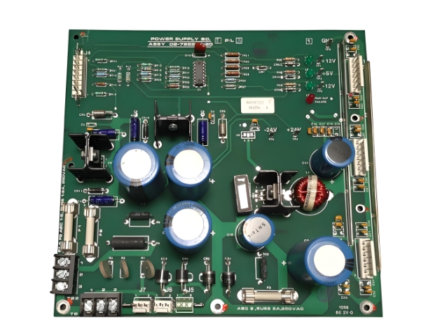
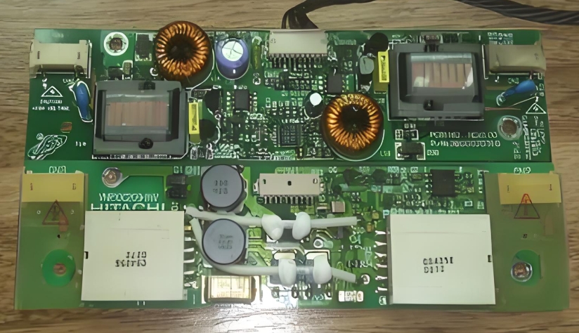
An LCD display screen PCB is a type of printed circuit board specifically designed to interface with an LCD panel. The PCB connects the LCD to the power supply, the signal-processing circuits, and any user input interfaces (e.g., touchscreen functionality). It provides both mechanical support and electrical connections that allow the display to function properly.
LCD technology itself works by manipulating light through liquid crystal molecules that change alignment when a voltage is applied. These crystals alter the light passing through them, creating an image on the screen. The PCB enables these electrical signals to be routed precisely to the individual pixels on the display, ensuring the correct image is formed.
Key Design Considerations for LCD Display Screen PCBs
The design of an LCD display screen PCB is influenced by several technical factors that impact the performance, durability, and functionality of the device. Below, we will explore the primary design considerations and how each one contributes to the final product.
1. Material Selection
The materials used in LCD display screen PCBs must be carefully selected to ensure the device functions effectively under varying environmental conditions. The primary materials used include:
- FR-4 (Flame Retardant 4): The most common PCB material, FR-4 is a composite made from woven glass and epoxy resin. It is cost-effective and has sufficient thermal and electrical properties for most standard LCD applications.
- Polyimide: In applications where flexibility is required, such as flexible or curved displays, polyimide substrates are used due to their excellent thermal stability and flexibility.
- High-Frequency Laminates (e.g., Rogers): For high-resolution and high-frequency displays, advanced laminates with low dielectric constants are chosen to ensure minimal signal loss and high-speed signal transmission. These materials are crucial for applications like high-definition displays in smartphones or medical devices.
2. Layer Count and Stack-up
The complexity of LCD display screen PCBs depends on the functionality required. Simple designs may use two-layer PCBs, while more advanced models require multi-layer designs to accommodate additional components such as capacitors, resistors, and signal routing.
- Two-Layer PCBs: Often used in basic applications where the design is straightforward, such as lower-resolution LCDs used in consumer electronics.
- Multi-Layer PCBs: More complex designs, such as those found in high-end LCDs, often require 4 to 10 layers or more. These PCBs provide additional routing space and can integrate more sophisticated components like power management circuits, touch sensors, and signal amplifiers.
3. Signal Integrity and Routing
Signal integrity is critical for LCD display screen PCBs, as high-frequency signals must be routed to each pixel with minimal interference. This is especially important for high-definition displays where pixel data is constantly being updated.
To maintain signal integrity, designers use techniques such as:
- Controlled impedance routing: This ensures that the PCB traces have a consistent impedance, minimizing reflections and signal loss.
- Use of via-in-pad: In complex designs, vias (holes in the PCB) are used to connect layers. Via-in-pad designs help maintain signal integrity in multi-layer PCBs by minimizing the electrical resistance between layers.
4. Thermal Management
Due to the dense concentration of electronic components and the high power consumption of modern LCDs, thermal management is essential to prevent overheating, which could damage sensitive components. Heat sinks, thermal vias, and copper pours are commonly used to dissipate heat efficiently.
Designers must also consider the thermal expansion coefficient (TEC) of materials, as mismatches between the PCB material and the LCD panel could lead to warping or cracking during temperature fluctuations.
5. Electromagnetic Interference (EMI)
LCDs are often used in environments with many other electronic devices, increasing the risk of electromagnetic interference (EMI). EMI can degrade the performance of the display, causing artifacts or screen flickering. To mitigate this, PCB designers use shielding techniques such as:
- Conductive layers that block unwanted signals.
- Ground planes to ensure a return path for current, reducing the risk of signal distortion.
The Physics Behind LCD Technology
1. Liquid Crystal Behavior
The core principle behind LCD technology is the use of liquid crystals. These crystals can change their alignment when subjected to an electric field, altering the passage of light. This phenomenon is known as the electro-optic effect. Liquid crystals do not emit light by themselves; instead, they modify the light passing through them.
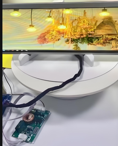
In an LCD, light is typically provided by a backlight—a layer of LEDs (light-emitting diodes) positioned behind the display panel. The liquid crystals act as shutters, controlling how much light passes through to form images. When voltage is applied to a particular pixel, the crystals align in a way that either blocks or permits light to pass through, creating dark or bright spots.
2. Polarization and Light Transmission
The liquid crystals in an LCD are sandwiched between two polarizing filters. The first filter polarizes the light, while the second filter only allows light that is aligned with the first filter to pass through. The liquid crystals twist and untwist when a voltage is applied, adjusting the amount of light passing through the second filter. This control over light transmission is how an LCD creates images.
Microstructural Differences in LCD Display PCBs
When comparing LCD display screen PCBs used in different applications, there are several key microstructural differences that impact performance:
- Pixel Density: High-definition (HD) displays require more complex PCB designs with finer traces to accommodate higher pixel densities. This involves advanced manufacturing techniques such as HDI (High-Density Interconnect) technology, which allows for smaller traces and vias, optimizing the use of space on the PCB.
- Flexibility: Flexible LCD display screen PCBs used in curved or bendable displays require the use of polyimide materials that can withstand mechanical stress without compromising signal integrity.
Data Visualization: Key Performance Metrics for LCD Display Screen PCBs
To visualize the performance of LCD display screen PCBs, consider the following interactive metrics:
- Signal Integrity vs. Trace Width: A line graph showing the relationship between signal loss and trace width for various materials used in LCD PCBs.
- Thermal Resistance Comparison: A bar chart comparing the thermal resistance of different PCB materials (e.g., FR-4, polyimide) under high-power conditions, showing how material choice impacts heat dissipation.
- Power Consumption vs. Resolution: A scatter plot showing the power consumption of LCD displays at different resolutions, highlighting how higher-resolution displays require more efficient PCB designs.
Applications and Industry Use Cases
1. Smartphones and Tablets
In smartphones and tablets, LCD display screen PCBs are used to support high-resolution, multi-touch screens. These devices require precise signal routing and efficient power distribution to manage the high-frequency signals driving the displays. The use of multi-layer PCBs helps manage the complexity of these systems, which often integrate additional features such as sensors and cameras.
2. Medical Devices
In medical devices, LCD displays are crucial for showing patient data and diagnostics. The PCB design for medical applications must ensure high reliability and compliance with regulatory standards. The signal integrity of LCD PCBs in these systems is paramount to ensure accurate readings and clear visuals.
3. Automotive Displays
In the automotive industry, LCD display screen PCBs are used in dashboard panels, navigation systems, and in-vehicle entertainment systems. These PCBs must be designed to withstand temperature extremes, vibrations, and electromagnetic interference, all while providing clear, real-time data to the driver.
Conclusion: Future Trends in LCD Display Screen PCB Design
The future of LCD display screen PCBs lies in the continuous advancement of materials, design techniques, and manufacturing technologies. As demand for higher-resolution, flexible, and energy-efficient displays grows, PCB designers will need to adopt new materials such as graphene and nanomaterials, optimize heat dissipation methods, and continue to refine signal integrity techniques.
In conclusion, the role of the LCD display screen PCB is critical to the success of modern electronic displays. By understanding the underlying physical principles, choosing the right materials, and addressing challenges such as thermal management and EMI, manufacturers can ensure that LCD technology continues to provide clear, reliable, and vibrant visual experiences in a wide range of applications.
Glossary:
- FR-4: A standard PCB material composed of fiberglass and epoxy resin.
- HDI: High-Density Interconnect, a PCB design technology used to create smaller, more complex circuits.
- Polyimide: A flexible and high-temperature-resistant material used in specialized PCB designs.
- Electro-optic Effect: A phenomenon where the alignment of liquid crystals changes in response to an electric field, controlling light transmission.
Interactive Elements:
- PCB Simulation Tool: An interactive tool that allows users to experiment with different PCB designs for LCD screens.
- Signal Integrity Calculator: A tool to visualize the impact of different trace widths and materials on signal quality in LCD PCBs.
