Introduction
Prototyping is a crucial step in the PCB development cycle, allowing engineers to test and validate their designs before mass production. However, high prototyping costs and minimum order quantity (MOQ) requirements can be barriers for startups, hardware developers, and research institutions. This article explores where to get free PCB prototypes service for 2-6 layer PCBs with zero MOQ, detailing the technical aspects, service quality, and cost-effectiveness of different providers.
Why Choose a Free PCB Prototype Service?
Before selecting a free PCB prototype service, it is essential to understand the key benefits:
- Cost Reduction: Eliminates initial expenses for small-scale prototyping.
- Design Validation: Allows early testing of circuit performance and manufacturability.
- Rapid Iteration: Faster turnaround for PCB design improvements.
- Zero MOQ Advantage: Ideal for small businesses and individual developers needing low-volume production.
Technical Considerations for 2-6 Layer PCB Prototyping
Stack-up Design: The number of layers affects signal integrity, impedance control, and EMI performance. Common layer configurations include:
- 2-layer PCB: Suitable for simple circuits, IoT devices, and power modules.
- 4-layer PCB: Offers better power distribution and noise reduction, used in high-speed digital applications.
- 6-layer PCB: Enhanced signal integrity for RF/microwave and high-frequency applications.
Materials & Manufacturing Specifications
| Parameter | 2-layer PCB | 4-layer PCB | 6-layer PCB |
|---|---|---|---|
| Material | FR4, Rogers | FR4, PTFE | FR4, High-Tg |
| Min. Trace Width | 4 mil | 3 mil | 3 mil |
| Min. Spacing | 4 mil | 3 mil | 3 mil |
| Min. Drill Size | 0.2 mm | 0.15 mm | 0.15 mm |
| Surface Finish | HASL, ENIG | HASL, ENIG | ENIG, OSP |

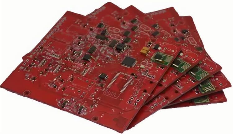
Where to Get Free PCB Prototypes?
1. JLCPCB Free Prototype Program
- Key Features: 5 free prototype PCBs (up to 2-layer, 100x100mm)
- Turnaround Time: 48 hours
- Supported Layers: 2 layers
- Best For: Hobbyists, students, and entry-level developers
2. PCBWay Free Prototyping Program
- Key Features: Free for small prototypes with community projects
- Turnaround Time: 3-5 days
- Supported Layers: Up to 4 layers
- Best For: Open-source hardware projects
3. Seeed Fusion Free PCB Prototyping
- Key Features: Free PCBs for approved projects
- Turnaround Time: 4-6 days
- Supported Layers: Up to 6 layers
- Best For: IoT, wearables, and smart devices
4. HXPCB’s No MOQ Prototyping Service
- Key Features: Zero MOQ, high-layer count PCBs
- Turnaround Time: 24-72 hours
- Supported Layers: 2-6 layers
- Best For: Industrial applications, AI hardware, and high-frequency circuits
How to Select the Best Free PCB Prototype Provider?
Choosing the right provider depends on the following factors:
- Technology & Material Support: Ensure the service supports FR4, Rogers, or PTFE materials based on your project needs.
- Layer Count & Stack-up Options: Verify whether 2-layer, 4-layer, or 6-layer PCBs are available.
- Design Rule Check (DRC) Standards: Check trace width, spacing, via sizes, and impedance control.
- Lead Time & Shipping Costs: Evaluate production speed and delivery reliability.
- Testing & Certification: Look for IPC Class 2/3 compliance and electrical testing options.

FAQ
Q: What does zero MOQ mean for PCB prototyping?
A: Zero MOQ means no minimum order quantity is required, making it ideal for developers needing just 1-5 boards for initial testing.
Q: Can I get free PCB prototypes with high-frequency materials?
A: Some providers offer free prototypes with Rogers or PTFE materials, but availability varies.
Q: How can I ensure my free PCB prototype meets quality standards?
A: Ensure the provider follows IPC-6012 standards and offers AOI (Automated Optical Inspection) and electrical testing.

