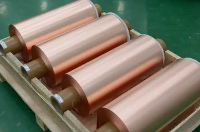
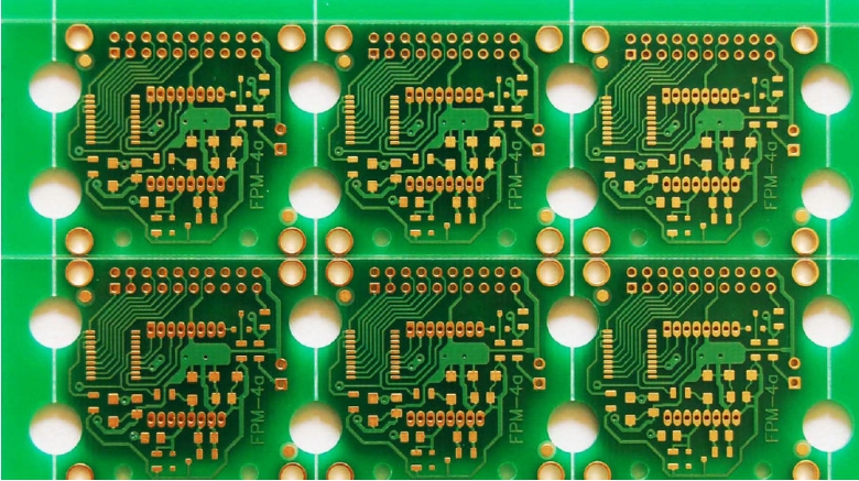
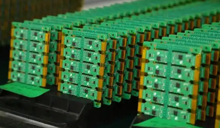
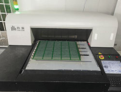
Consumer electronics

Consumer electronics PCB manufacturing

HXPCB is a manufacturer with more than ten years of experience in the PCB industry. We provide one-stop PCB manufacturing and assembly services. We provide high-quality consumer electronics PCBs, including design, layout and final testing and packaging services. We have enough confidence in our product quality, our production technology and our services. Please tell us your needs and we will do our best to solve them for you.

Product Introduction:
Consumer electronics PCBs are printed circuit boards used in a variety of consumer electronic devices, including smartphones, tablets, TVs, home appliances, portable devices, audio systems, etc. Consumer electronics circuit boards require powerful, cost-effective and compact designs to meet the high frequency, high density and rapidly developing technology requirements in daily use.

Consumer Electronics

Consumer electronics PCB display

Common Materials for Consumer Electronics PCBs

PCB material (FR-4)

Substrate materials

1. Glass epoxy resin (FR-4): low cost, suitable for mass production, widely used in mobile phones, computers, etc.2. Ceramic substrate: used for high-frequency communication equipment, such as radio frequency identification (RFID) and microwave equipment.
3. Metal substrate: such as aluminum substrate and copper substrate, used for equipment that requires high heat dissipation, such as LED lights and electric vehicles.

PCB production materials (copper foil)

Copper foil and solder resist

1. Thickness at 35μm: suitable for consumer electronics, low conductor loss.
2. Thickness at 18μm: used for high-frequency signals or miniaturized equipment.
3. Water-based solder resist: easy to handle, environmental protection issues need to be paid attention to.
4. Solder patible ink: environmentally friendly and suitable for wave soldering.
5. UV curing coating: used for high density or special processes.

PCB material (conductive polymer)

Antistatic coating

1. Conductive polymer: suitable for high-density boards.

2. Carbon nanotubes: good conductivity, high cost.

3. Organic matter + carbon black: low cost, suitable for general needs.

PCB high frequency board (Rogers ro4000)

High-frequency materials and special materials

1. PTFE: low dielectric constant, used in high-speed digital and RF applications.

2. Flexible boards and rigid-flex boards: used in wearable devices, providing bending and folding functions.

Main features of consumer electronics PCBs

High-density design

Consumer electronics products place high demands on the spatial structure of printed circuit boards, and usually require high-density design to accept more circuits and components with limited space.

Multi-layer structure

In order to save space and improve performance, consumer electronic panels usually adopt a multi-layer structure, which can effectively reduce the difficulty of wiring and improve signal transmission efficiency.

High-frequency power supply

Many consumer electronic devices, such as smartphones and Wi-Fi routers, must support high-frequency signals. Therefore, choosing the right materials and design methods are crucial to ensure signal integrity and reduce losses.

Thermal management

With the increase in power consumption of CPUs and other components, thermal management has become a major challenge in PCB consumer electronic design. Choosing the right materials and design methods are both important.

Lightweight design

Many consumer electronic products require very sophisticated PCB designs to be used in modern lightweight devices.

High reliability

Consumer electronic products are usually mass-produced and require high reliability to ensure long-term stable operation, especially under harsh conditions such as high temperature and humidity.

Consumer electronics PCB design requirements

Signal defect consideration
The signal transmission quality must be considered during design, and signal loss due to line impedance mismatch, crosstalk and other problems must be avoided.

Efficient power management
As the functions of electronic devices increase, power management becomes more and more complex, so efficient and stable power supply design is required.

EMI/EMC management
Electronic devices must comply with electromagnetic interference (EMI) and electromagnetic compatibility (EMC) standards, so it is particularly important to carry out detailed design to reduce interference.

Consumer electronics PCB application areas

Smart home devices

Wearable devices

Home appliances

Smartphones

Consumer electronics PCB assembly process

The assembly of consumer electronics PCBs (printed circuit boards) is a meticulous process that requires extreme precision and expertise. From assembly to final inspection, each step plays a vital role in ensuring the end product meets the highest standards of quality and reliability. Here, we take a deep dive into the PCB assembly process, gaining an in-depth understanding of each stage — while also considering the human factors involved to achieve better results.

Step1:Material Preparation and Soldering Preparation

Consumer Electronics PCB

1.Material Preparation

All electronic components come together here. From tiny resistors and capacitors to large chips and connectors of various shapes, workers organize and sort the components into designated bins based on the specific needs of the production order. An experienced assembler, upon receiving the production order, will immediately check the inventory of all components to ensure that nothing is missing or incorrect.

Consumer Electronics PCB

2.Soldering Preparation

On the PCB carrier, a layer of solder paste is first applied to the designated solder pads. While this step may seem simple, it plays a crucial role in the overall quality of the soldering process. The solder paste undergoes strict quality checks, including testing for viscosity, metal content, and other factors. In some factories, manual application is preferred, especially for complex PCB designs. Workers use specialized brushes to carefully apply the paste to each pad, ensuring the right amount is applied—not too much and not too little.

Step 2: SMT (Surface-Mount Technology) Placement

SMT equipment

1.Machine Inspection

The PCB is placed on the conveyor belt of the SMT (Surface-Mount Technology) machine. Before the actual placement of components begins, the machine automatically scans the PCB’s fiducial marks to perform coordinate alignment, ensuring that each component is placed accurately.

Consumer Electronics PCBA

2.Automatic Placement

The SMT machine begins its operation. A high-speed suction arm precisely picks up components from the component trays and places them onto the PCB at a speed of several millimeters per second. This process is so precise that each step is measured down to the hundredth of a millimeter. While machines dominate this process, workers still manually adjust special-shaped components, especially when there are large numbers or a variety of components.

Step 3: THT (Through-Hole Technology) Soldering

Consumer Electronics PCB Assembly

1.Component Insertion

For components that require THT (Through-Hole Technology) soldering, workers manually insert the component leads into the holes on the PCB. The key here is controlling the force; too little pressure will cause the component to be unstable, while too much pressure could damage the PCB or the component itself.

Consumer Electronics PCB Assembly

2.Wave Soldering

The PCB is then sent through the wave soldering machine, where molten solder waves evenly cover the component leads and pads, forming solid solder joints. While this step is automated, it still requires experienced engineers to adjust the solder temperature, speed, and wave form to ensure optimal soldering quality. In dense areas with many components, workers may need to manually remove excess solder or fix any defects

Step 4: Manual Assisted Assembly

Introduction to the Process Characteristics and Workflow of Selective Soldering for PCB Circuit Boards

1.Hand Soldering

For specialized components, such as connectors with metal housings or very large chips, workers perform manual soldering. Wearing anti-static wristbands and using adjustable temperature soldering irons, they carry out precise soldering operations under a microscope. This process requires great patience and focus, as these components are often crucial to the overall circuit, and the quality of the soldering directly impacts the product’s performance.

PCB manual assembly

2.Component Installation

Some parts, such as battery clips, switches, and LEDs, cannot be assembled using SMT or THT processes, and are installed manually. Although these parts seem simple, they are critical to the user experience, and even the smallest installation error could lead to product failure.

Step 5: Testing and Inspection

PCB automatic optical inspection

1.Automated Optical Inspection (AOI)

The assembled PCB is sent to the AOI machine, which uses high-speed cameras to scan each solder joint for issues such as short circuits, open circuits, or solder defects. This is a critical quality control step, but even so, experienced inspectors are needed to review the AOI results, particularly for complex solder joints where the machine may make false judgments.

PCB manual inspection

2.Manual Inspection

Sometimes, the AOI system may miss issues, especially with hidden solder joints or special components. In these cases, it is up to skilled workers with years of experience to manually inspect each potential trouble spot to ensure every solder joint is perfect. Their keen eyes help catch any defects that may otherwise go unnoticed.

This process combines the benefits of automation with the expertise of skilled workers to ensure that each PCB assembly meets the high standards required for reliable consumer electronics. The balance between machine efficiency and human precision results in a high-quality end product that meets both functional and aesthetic requirements.

Our Manufacturing and Assembly Capabilities


CategoryDetails
Layer Count and Board TypesSingle-layer to 20-layer PCBs (standard), up to 64 layers for advanced designs. <br> Rigid, flexible, and rigid-flex PCBs for diverse applications.
Material OptionsFR-4 (standard/high TG), flexible substrates (Polyimide), high-frequency materials (Rogers, PTFE).
Precision and DensityMinimum trace width/spacing: 0.075 mm (3 mils). <br> Minimum hole diameter: 0.1 mm (laser drilled). <br> HDI capability: microvias, blind and buried vias.
Board Thickness0.4 mm to 3.2 mm, supporting ultra-thin boards for lightweight designs.
Surface Finish OptionsENIG, OSP, HASL, Immersion Silver/Gold, and more.
Quality AssuranceAOI, X-Ray, Flying Probe Testing, Electrical Testing; ISO 9001, RoHS, UL certifications.
Category Details
Component Handling Support for 01005 components, BGA, QFN, CSP packages.  Placement accuracy: ±25 µm for SMT components.
Production Volume From small-batch prototyping to high-volume production.
Assembly Technologies SMT with lead-free soldering; THT for hybrid assembly.
Testing and Validation Functional Testing (FCT), In-Circuit Testing (ICT), reliability testing (aging, thermal cycling, etc).
Category Details
Smartphones and Tablets HDI PCBs, flexible circuits for compact, high-performance designs.
Wearable Devices Ultra-thin, flexible boards for lightweight and durable designs.
Smart Home Devices IoT PCBs optimized for connectivity and low-power operation.
Audio and Video Systems Boards designed for high signal integrity and superior output.

Consumer Electronics PCB Assembly Services

HXPCB provides consumer electronics PCB assembly services. We provide technical support to our customers with more than ten years of experience. Whether it is a manufacturing problem, assembly problem or other problems, we will help customers solve the difficulties they encounter. We have our own rich and complete supply chain and production line, professional engineers and enthusiastic salesmen who are dedicated to answering your questions. Contact us now.

About our advantages

Functional test guarantee

Supports multiple detection methods such as ICT (circuit test), FCT (functional test), aging test, etc

High-precision manufacturing capabilities

Support advanced laser drilling, blind and buried hole technology and fine line width/line spacing manufacturing processes.

Fast delivery

Efficient production process and quality management, quickly respond to customer needs from proofing to mass production.

Strong assembly capabilities

Support the assembly of flexible boards, rigid-flexible boards and complex multi-layer boards, and provide one-stop services from parts procurement to test assembly.

Technology and assembly equipment

Supports technologies such as automatic welding, automatic dispensing and selective wave soldering, and supports precision placement of miniaturized and high-density components (BGA, CSP, QFN).

Small and large quantities

Support customers to place small and large batch orders, one-stop PCB manufacturing and assembly services.

FAQ

Frequently Asked Question

FR-4 is the standard material for most consumer electronics due to its balance of cost and performance. For lightweight and compact devices, polyimide-based flexible substrates are ideal. High-frequency materials like Rogers or PTFE are used in devices requiring high-speed data transmission, such as routers or advanced audio systems.

Consumer electronics commonly use rigid PCBs for durability, flexible PCBs for lightweight and compact designs, and rigid-flex PCBs for advanced applications requiring both flexibility and rigidity. High-Density Interconnect (HDI) boards are often used for compact, high-performance devices like smartphones and tablets.

ENIG (Electroless Nickel Immersion Gold) is preferred for its durability and excellent conductivity. OSP (Organic Solderability Preservative) is cost-effective for short-life products. Immersion Silver or Immersion Tin may also be used based on specific application needs.

Durability is ensured by using flexible materials with high fatigue resistance, selecting appropriate surface finishes to prevent oxidation, and designing with reinforced edges or stiffeners where necessary. Rigorous environmental testing such as thermal cycling and bending tests is also conducted.

 Lead times vary depending on complexity. For standard boards, prototyping typically takes 5–7 days, while mass production can take 2–4 weeks. HDI and rigid-flex boards may require additional time due to their complexity.

Quality is verified using AOI (Automated Optical Inspection), Flying Probe Testing, X-Ray Inspection, ICT (In-Circuit Testing), and Functional Testing (FCT). For consumer electronics, additional tests like thermal cycling, aging tests, and environmental exposure tests are also conducted.

Do you need any help?

HXPCB manufacturers have always been

HXPCB Manufacturer: Blog

News & Articles

multi-layer PCB

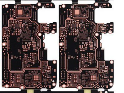
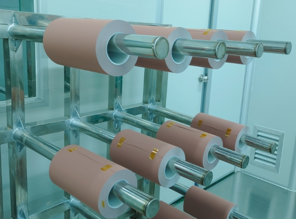
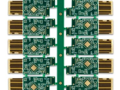
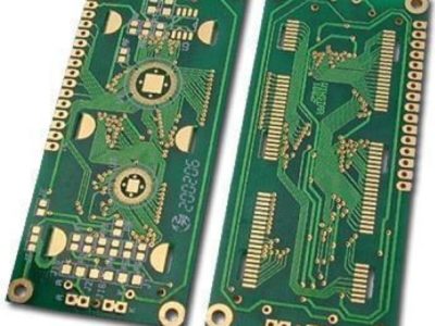
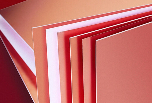
High-end design, multi-layer PCB internal structure and experience sharing

Read More

PCB detection steps

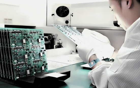
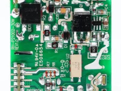
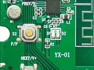
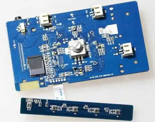
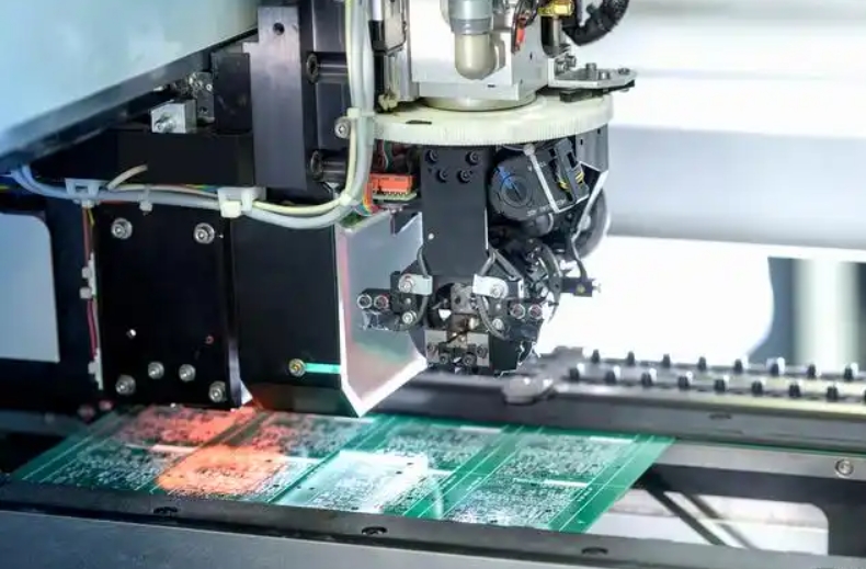
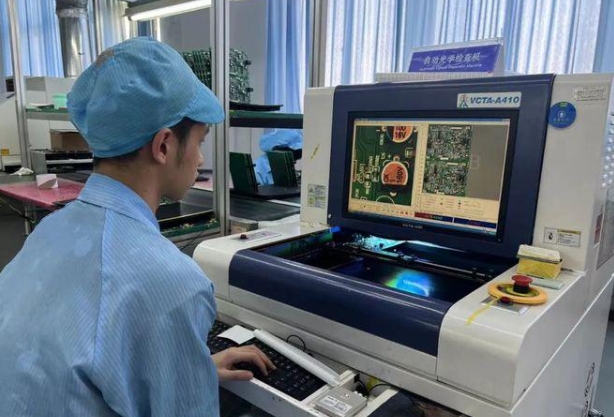
PCB (Printed Circuit Board) inspection is an important part of ensuring product quality, performance and reliability.

Read More

PCB Manufacturing and Assembly

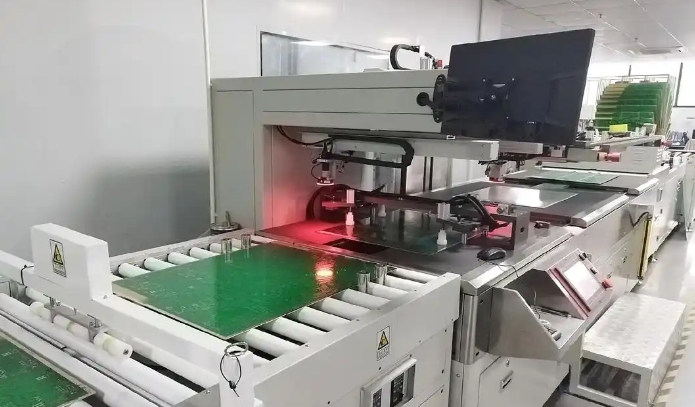
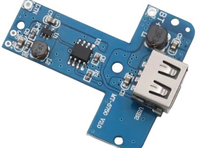
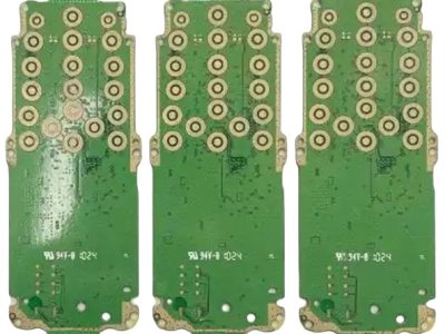
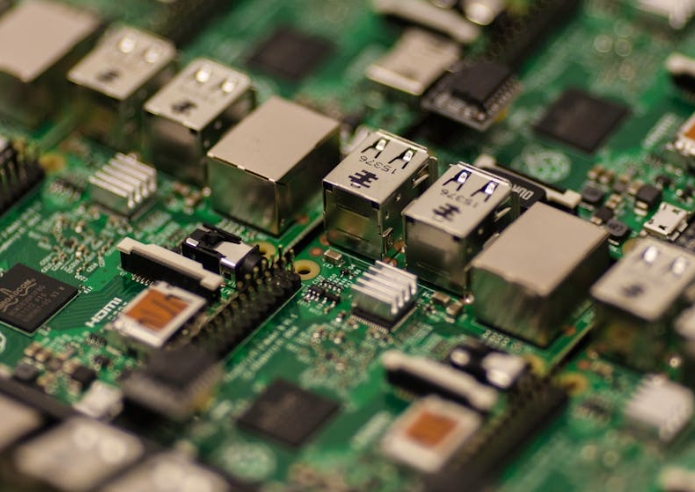
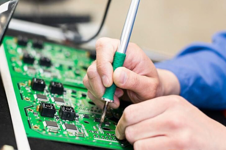
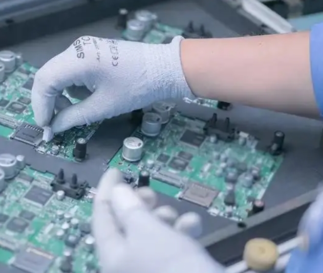
Printed circuit boards (PCBs) play a vital role in connecting and supporting various electronic components. With

Read More
ja