Printed circuit boards (PCBs) play a vital role in connecting and supporting various electronic components. With the continuous improvement of the performance requirements of electronic products, PCB manufacturing and assembly technology has been continuously developing and has long become an important part of the electronics industry. Next, let’s take a look at the manufacturing and assembly process of PCBs.
1. PCB design and layout
PCB design involves more than just placing components; signal integrity, power integrity, and thermal management must also be considered. In the design stage, first select the appropriate materials, determine the circuit layout, and perform electrical simulation to ensure that the design meets the functional requirements of the product.
PCB design tools such as Altium Designer and Cadence Allegro provide powerful functions for schematic capture, routing, and generating Gerber files. Gerber files are standard input files for PCB production, which contain the graphic data of the circuit board. Manufacturers use this file to perform PCB manufacturing and assembly. The following are Altium Designer and Cadence Allegro tools.

2. Material selection for PCB
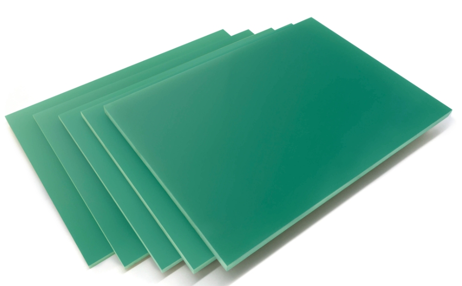
The choice of materials directly affects the performance and manufacturing cost of PCBs. Common PCB materials include FR-4, aluminum substrates, ceramic substrates, etc. FR-4 is widely used in standard electronic products because of its low cost and good electrical performance. For high-frequency or high-speed circuits, high-frequency materials PTFE or Rogers may be the best choice, which can minimize signal loss and increase transmission speed. When facing high-power applications, we usually choose aluminum substrates because they have excellent thermal conductivity and help dissipate heat. For applications that require high temperature resistance, materials such as polyimide (PI) are ideal. Of course, there are differences between the same materials. For example, the same material also has different series models. These different models of the same material are basically not much different, but the gap can be felt when facing some refined applications.
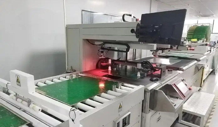
3. PCB Manufacturing Process
PCB manufacturing usually involves several key steps:
Copper clad board preparation: The process starts with a copper clad board, which has a layer of copper foil on both sides. Through chemical etching or laser ablation, unwanted copper is removed, leaving the desired circuit pattern.
Drilling and hole processing: Holes need to be drilled on the PCB according to the design for component leads or interconnections. The diameter, position and quality of the holes are critical to ensure the integrity and electrical performance of the solder joints.
Surface treatment and solder mask: To improve solderability, PCBs are usually surface treated. Common surface treatment methods include immersion gold, hard gold plating, gold finger plating, OSP (organic solderability preservative), etc. Proper surface treatment can improve solder quality and electrical performance.
4. PCB assembly process
The assembly process is a key step in the manufacture of electronic products. It usually involves component placement and soldering.
Component placement: With the widespread adoption of surface mount technology (SMT), most electronic components are mounted on the surface of PCBs. This is usually achieved by automatic machinery such as pick-and-place machines, which provide high-speed, high-precision placement, greatly improving production efficiency.

Soldering: Soldering is one of the most critical processes in PCB assembly. Common soldering methods include wave soldering, reflow soldering, and hand soldering. Reflow soldering is commonly used for surface mount components, which heats the solder paste to form a strong electrical connection between the component and the PCB.
Functional testing and inspection: After soldering, the PCB undergoes functional testing to check electrical continuity and normal operation of the circuit. The test ensures that each solder joint is intact and the electrical components operate as expected. Additionally, technologies such as automated optical inspection (AOI) and X-ray inspection are used to detect potential defects such as opens, shorts, and bad solder joints.
