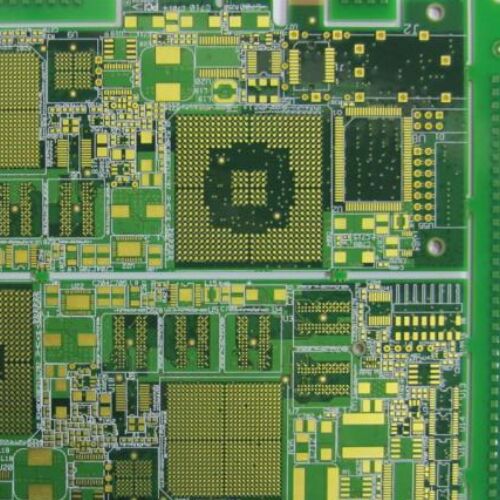
So, what knowledge is essential for routing multilayer PCBs? PCB routing involves laying out printed conductors based on the PCB schematic, wire list, and required wire width and spacing.
- Simplicity in Routing: Routing should be as simple as possible while meeting requirements. The preferred order for routing methods is single-layer, double-layer, and then multilayer.
- Grounding and Shielding: Ground lines should be placed next to input lines in analog circuits for shielding. Conductors on the same layer should be evenly distributed, and the conductive areas on each layer should be relatively balanced.
- Smooth Transitions: Signal lines should change direction using diagonal or smooth curves to avoid electric field concentration, signal reflection, and additional impedance.
- Separation of Circuits: Digital and analog circuits should be separated in routing to prevent interference. Ground lines should be placed between signal lines of different frequencies to avoid crosstalk. For testing convenience, necessary breakpoints and test points should be included in the design.
- Short and Direct Connections: Connections for grounding and power supply should be as short and direct as possible to reduce internal resistance.
- Orthogonal Routing: Conductors on adjacent layers should be perpendicular to each other to minimize coupling. Avoid aligning or paralleling conductors on different layers.
- Equal Length for High-Speed Circuits: For high-speed circuits, multiple I/O lines, as well as I/O lines for differential amplifiers and balanced amplifiers, should be of equal length to avoid unnecessary delays or phase shifts.
- Thermal Isolation for Pads: When connecting PCB pads to large conductive areas, use thin conductors with a length of at least 0.5mm for thermal isolation. The width of these thin conductors should be no less than 0.13mm.
- Edge Clearance: Conductors closest to the edge of the SMB (Surface Mount Board) should be at least 5mm away from the edge. Ground lines can be closer to the edge if necessary.
- Power and Ground Routing: For double-sided SMBs, power and ground lines should be routed near the edges and distributed on both sides. For multilayer SMBs, power and ground layers can be set internally, connected to power and ground lines on each layer through vias. Large conductive areas and power/ground lines on inner layers should be designed in a grid pattern.
By mastering these principles, you can effectively route multilayer PCBs, ensuring optimal performance and reliability.

