- Schematic design: Lay a solid foundation for hardware development
Functional requirements and module division:
In-depth understanding of product functional requirements and performance indicators to ensure that the design meets practical applications.
Disassemble the overall requirements into functional modules to reduce circuit complexity and facilitate subsequent layout and maintenance.
Component selection:
Select appropriate components such as processors, sensors, etc. according to functional requirements.
Comprehensively consider packaging, cost and reliability to ensure that components operate stably in the system.
Schematic drawing and inspection:
Use EDA tools to draw schematics and add correct packaging information.
Continuously check electrical rules to ensure that signal connections are correct.
After completion, check against requirements and specifications to ensure that there are no omissions or errors.

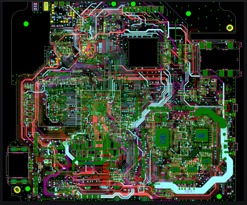
- PCB layout: Convert the design into an actual circuit board
PCB stacking structure:
Select an appropriate stacking structure based on product complexity, signal frequency and cost.
Rationally allocate power layers and ground layers to improve anti-interference capabilities.
Component layout:
Functional partitioning, reduce signal crossing, and keep the routing clean.
Pay attention to heat dissipation and space, and reserve heat dissipation channels for heat-generating devices.
Combined with mechanical structure information, ensure that the hole position, edge and key device layout are reasonable.
Routing principles and signal integrity:
Separate strong and weak electricity to avoid mutual interference.
High-speed interface uses differential routing to ensure signal integrity.
Prioritize the allocation of key signal paths to ensure timing requirements.
Maintain the integrity of the reference plane to reduce electromagnetic radiation and crosstalk.
Power and ground design:
Choose a suitable grounding strategy, such as single-point grounding or multi-point grounding.
Arrange decoupling capacitors to reduce power supply interference.
Reasonably design power channels and line widths to prevent voltage drops and overheating.
III. EMI/EMC design and electromagnetic compatibility
Sources of electromagnetic interference:
Internal interference: interference from high-frequency digital circuits, switching power supplies and other modules.
External interference: RF radiation from peripheral equipment or environment, etc.
Methods to reduce EMI interference:
Shielding and isolation: Shield sensitive signals and strong noise sources.
EMC filter: Add filters to the power or data line end to suppress interference.
Reasonable ground line division: separation of analog ground, digital ground, and power ground to reduce noise coupling.
Capacitor and RC filtering: Add filtering networks at sensitive nodes to alleviate interference.
EMC testing and certification:
Perform CE, FCC and other electromagnetic compatibility certification tests to ensure that the product meets the requirements.
Perform pre-compatibility testing in advance to optimize PCB design.
- Thermal design and mechanical structure considerations
Heat dissipation strategy:
Design reasonable heat dissipation channels for high-power devices, such as copper skin area heat dissipation, heat sinks, etc.
Consider the thermal path to ensure effective heat transfer and diffusion.
Component height and layout:
Combined with the shell structure to avoid device interference.
Leave enough space for plug-in components or operating devices.
Reserve test points for subsequent detection and troubleshooting.
Production feasibility (DFM):
Pay attention to production requirements such as device spacing and via size.
Consider mounting direction, solderability and automated detection requirements.
- Production process and quality control
PCB manufacturing:
Output Gerber files, drilling files, etc. to PCB manufacturers.
Communicate details such as board type and board thickness to understand process limitations.
SMT mounting and post-soldering:
Perform SMT programming according to the package type and set the reflow soldering temperature curve.
Use AOI and X-Ray to check for soldering defects.
Use wave soldering or manual soldering for plug-in components.
Testing and debugging:
Perform ICT testing to detect short circuits, open circuits, etc. on the circuit board.
Verify the functional modules and troubleshoot problems in the power-on state.
Perform safety and reliability testing to ensure that the product meets the requirements.

VI. Summary and improvement direction
Continuous iteration:
Through multiple rounds of debugging and improvement, balance performance, cost, process and reliability.
Collect test data and user feedback to optimize circuit and layout details.
Combination of theory and practice:
Be familiar with circuit analysis methods and PCB design specifications to quickly locate problems.
Accumulate experience in practice to deal with production restrictions, noise coupling and other problems.
Master advanced tools and technologies:
Learn cutting-edge technologies such as high-speed circuit design and simulation to reduce later rework.
Focus on ECAD and MCAD collaborative design, shorten R&D cycle and improve quality.
Advantages of Hongxin Circuit PCB(HXPCB) Manufacturer:1-6 layer PCB free proofing services
Hongxin Circuit PCB Manufacturer: Provide «high-quality, customized» PCB services from production optimization, quality control, etc. The company has always taken providing highly flexible and fast-response production services as its core competitiveness. The production cycle is flexible and diverse, ranging from 12 hours to 72 hours, accurately matching customers’ diverse urgent delivery needs. Whether it is small-batch customization or large-scale mass production, HXPCB can handle it with ease, showing excellent production flexibility and adaptability. The product variety is rich and distinctive, covering 2-layer to 30-layer FR-4 PCB, high-performance IMS PCB, high-density HDI board and rigid-flexible board, etc., which are widely used in various electronic equipment fields. HXPCB has always adhered to the concept of professionalism, efficiency and innovation, continued to increase R&D investment, optimized production processes, and is committed to providing customers with high-quality and high-performance printed circuit board products. Its products have penetrated into many key fields such as instrumentation, industrial control, communications, automotive electronics, medical electronics, security, power appliances, consumer electronics, etc., providing solid circuit support for the innovative development of these industries, and won wide praise and trust.

In summary, hardware development is a complex process involving multiple links, which requires comprehensive consideration of schematic design, PCB layout, EMI/EMC design, thermal design and mechanical structure. Through continuous iteration, combining theory with practice, and mastering advanced tools and technologies, product quality can be continuously improved. At the same time, choosing a PCB manufacturer with high-quality customized services is also the key to ensure the success of product development.

HXPCB 2-30 layer PCB manufacturing (1-6 layer PCB free proofing services)

