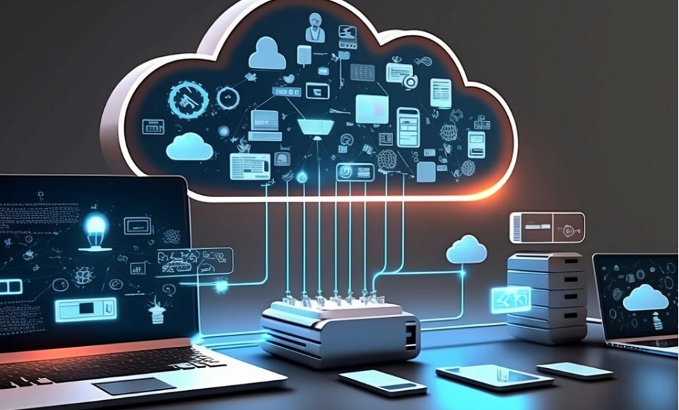
IoT PCB
HXPCB provides IoT PCB manufacturing
The term «Internet of Things» was first proposed by Kevin Ashton in 1999 to describe a system that connects devices through RFID (radio frequency identification) and the Internet. In the 21st century, the application areas of the Internet of Things have gradually expanded. From the initial logistics and warehouse management to smart homes, industrial automation, medical monitoring, smart agriculture and other fields, the Internet of Things technology continues to develop.
As a strong competitor in the PCB industry, HXPCB provides professional Internet of Things PCB manufacturing and services. We have rich experience and advanced technology and a team of hundreds of people. We support the design and manufacturing of multi-layer boards, flexible boards and rigid-flex boards, which can meet the needs of Internet of Things devices with reasonable layout, low power consumption and high reliability. HXPCB also provides comprehensive prototype development, fast delivery, and strict quality control to ensure the performance and sustainable growth of Internet of Things devices. We have been working hard for customer satisfaction. Please let me serve you, dear you.
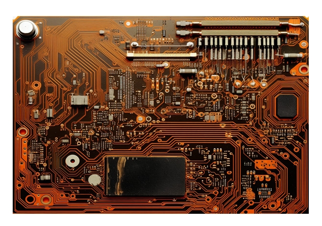
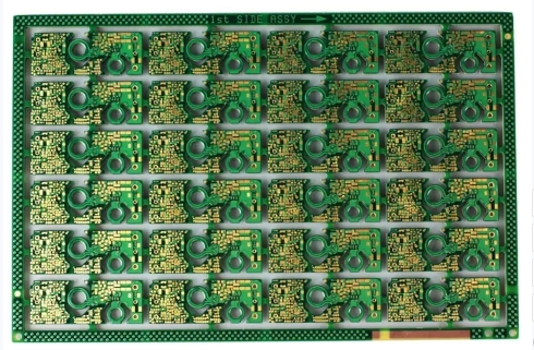
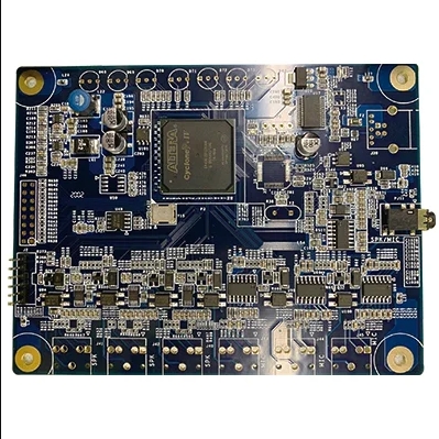
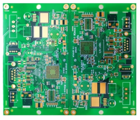
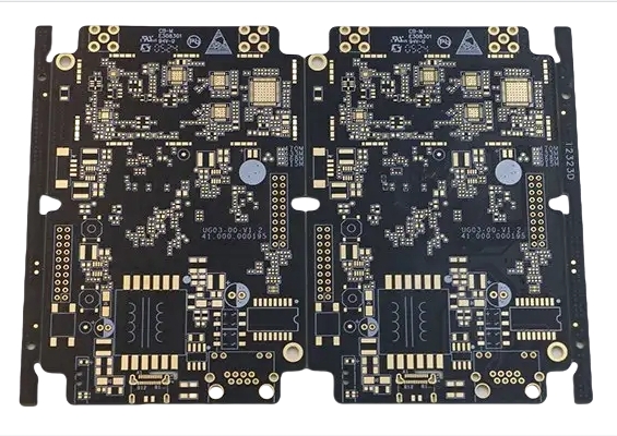
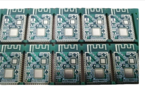
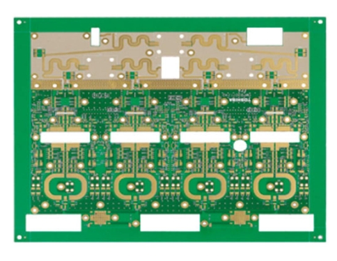
LOT PCB sample display
What is an IoT PCB?
IoT PCB is a specialized PCB designed to support devices in the IoT ecosystem. IoT PCB is the backbone of IoT devices, enabling connectivity, data processing, and communication between smart devices and the network. They typically integrate features such as wireless communication modules (e.g. Wi-Fi, Bluetooth, Zigbee), sensors, microcontrollers, and power management systems.
Application of IoT PCB
Healthcare
IoT PCB is very important in the healthcare industry and can be used in health monitoring equipment as well as medical devices such as wearable devices and remote monitoring systems.
Agricultural irrigation
IoT PCB is widely used in agricultural applications such as smart irrigation and precision seeding. Implementing agricultural production standardization and improvement greatly improves agricultural planting efficiency and benefits.
Traffic Guide
In the field of intelligent transportation, IoT PCB is used in traffic signals, traffic navigation equipment, parking systems, etc.
Smart Home
IoT PCB can be used in smart home devices such as smart lights, smart sockets, smart glasses, etc. Home comfort and living standards have been greatly improved.
Industrial Automation
IoT PCB is used in industrial automation fields such as intelligent control, logistics management, and intelligent manufacturing. Make the manufacturing process streamlined and efficient.
Smart City
IoT PCB can be used in smart city construction to realize scenes such as automatic street lights, parking lots, and parking lots. Add beauty to the city and bring comfort to the people.
Our Manufacturing Capabilities
| Parameter Category | Capability Parameters | Description |
| Layers | 1-12 Layers | Supports up to 12-layer IoT PCBs. |
| Thickness | 0.2-6.0 mm | PCB thickness ranges from 0.2 mm to 6.0 mm. |
| Min Line Width/Spacing | 2.5 mil/2.5 mil | Minimum line width and spacing of 2.5 mil. |
| Materials | FR-4, High-Tg materials, Flexible PCB, High-frequency materials | We use FR-4, High-Tg materials, FPC, and specialized high-frequency materials. |
| Surface Finish | Lead-free HASL, ENIG, Immersion Tin, OSP | Lead-free HASL, ENIG, Immersion Tin, OSP finishes available. |
| Hole Diameter | 0.15-6.0 mm | Hole diameters range from 0.15 mm to 6.0 mm. |
| Impedance Control | ±5% | Impedance control tolerance within ±5%. |
| Thermal Resistance | Operating temperature range: -40°C to 150°C | Operating temperature range from -40°C to 150°C. |
| Soldering Processes | Lead-Free Soldering | Compliant with industry standards for lead-free soldering. |
| Testing Capabilities | Electrical Testing, AOI, X-Ray Inspection, Functional Testing | Comprehensive testing including electrical, AOI, X-ray, and functional testing to ensure quality and reliability. |
| Certifications | RoHS, REACH, ISO 9001 | Certified with RoHS, REACH, and ISO 9001. |
HXPCB Services
PCB Design Services
Technical Support and After-sales Service
PCB Manufacturing Services
PCB Assembly Services
Prototype Manufacturing and Small Batch Production
Quality Control and Testing
Global Logistics and Delivery
Ultra-fast response
FAQ
Frequently Asked Question
IoT PCBs are widely used in smart homes, smart transportation, smart health, and smart agriculture, supporting remote control and data transmission for various devices.
The minimum line width and spacing for IoT PCBs are typically 2.5 mils, which supports high-density designs.
Impedance control in IoT PCBs is typically managed within a ±5% tolerance to ensure signal integrity and reliability.
High-frequency signals in IoT PCBs are managed using high-frequency materials (like PTFE and High-Tg materials) to minimize signal loss and ensure stable signal transmission.
Common surface finishes include lead-free HASL, ENIG, immersion tin, and OSP, depending on the connectivity requirements.
The typical layer count for IoT PCBs ranges from 1 to 12 layers, depending on the complexity and requirements of the device.
Common materials used for IoT PCBs include FR-4, High-Tg materials, Flexible PCBs (FPC), and high-frequency materials to ensure stable signal transmission.
The maximum thickness for IoT PCBs can reach up to 6.0mm, depending on the application requirements.
IoT PCBs typically operate within a temperature range of -40°C to 150°C, suitable for extreme environmental conditions.
Functional testing for IoT PCBs includes electrical testing, Automated Optical Inspection (AOI), X-ray inspection, and other tests to ensure the quality and performance of each PCB.