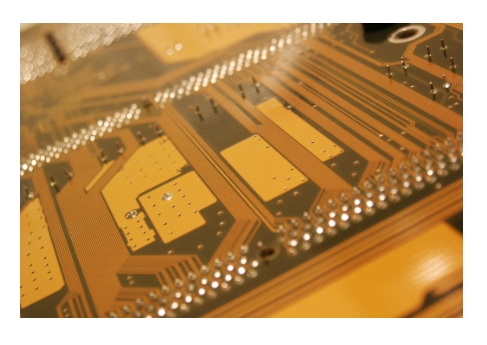
multi-layer PCB
High-end design,
Read MoreHXPCB focuses on the research and development of ultra-large size circuits board, multi-layer PCBs, metal-based PCBs, rigid-flex high-frequency PCBs, HDI PCBs, and related processes. We offer comprehensive services, including PCB design, prototyping, processing, and assembly.
Flexible Circuit Board (FPC) is a printed circuit board that can be bent and folded. It is designed with high flexibility to adapt to complex shapes and compact spaces. Unlike traditional rigid PCBs, FPCs are made of flexible substrates such as polyimide (PI) or polyester (PET). This feature makes it ideal for devices that require high density, lightweight, and reliable interconnection.
1. Strong flexibility
Flexible circuit boards can be bent, folded, twisted, and even curled to accommodate complex layouts in three-dimensional space. This flexibility makes it ideal for space-constrained applications such as smartphones and wearable devices.
2. Efficient heat dissipation
Flexible circuit boards have excellent thermal conductivity and can effectively dissipate heat, especially in multi-layer flexible circuits. This makes them suitable for applications with high heat dissipation requirements, such as LED modules and high-frequency communication equipment.
3. High reliability
Flexible circuit boards can withstand multiple bends, dynamic movements, and mechanical stresses without affecting their electrical performance. This makes them perform well in scenarios that require repeated folding, such as folding screen mobile phones and robotic arm equipment.
4. Lightweight design
FPC uses flexible materials (such as polyimide or polyester), which are usually only tens of microns thick and weigh much less than rigid PCBs. This is especially important for electronic devices that focus on lightweighting (such as drones and smartphones).
5. High space utilization
Since FPC can use extremely narrow wire widths and spacing (usually as low as 25 microns or less), it can achieve high-density wiring in a limited area, which is suitable for high-performance electronic products.
| Material Type | Material Description | Thickness Range |
| 1. Substrates | ||
| Polyimide (PI) | 12.5 – 50 μm | |
| Polyester (PET) | 5 – 25 μm | |
| Polyimide Film | 12.5 – 50 μm | |
| Polyester Film | 5 – 25 μm | |
| 2. Conductive Layer | Copper Foil | 17 – 70 μm |
| 3. Covering Films | Polyester Resin | 12.5 – 50 μm |
| Polyurethane | 10 – 30 μm | |
| 4. Reinforcement Materials | ||
| Glass Fiber Cloth | 0.05 – 0.2 mm | |
| PI Reinforcement | N/A | |
| PED Reinforcement | N/A | |
| Stainless Steel (Metal Reinforcement) | N/A | |
| 5. Auxiliary Materials | ||
| Cleaning Solutions | N/A | |
| Developing Solutions | N/A | |
| Etching Solutions | N/A |
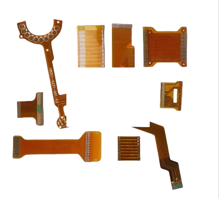
1. Design and layout
The production of flexible circuit boards starts with circuit design and layout. The circuit diagram is laid out through professional design software to optimize the line width, distribution and arc area design. The generated GERBER file will be used as a basic reference for production.
2. Material selection
Select the substrate of the flexible circuit board, such as polyimide (PI) or polyester (PET), and select the foil copper thickness, cover film type and adhesive according to actual needs to ensure that the material meets the flexibility and performance requirements of the product.
3. Copper circuit production
The core of the flexible circuit board is located in a copper circuit pattern.
3.1 Application of photoresist:
Coat the surface of the copper foil with photoresist, and evenly form a photosensitive layer, and transfer the circuit pattern to the photoresist through a mask.
3.2 Contact and development:
After exposure, use an exposure agent to reach the uncured photoresist, leaving the area of the circuit design.
3.3 Precision processing:
Use chemical solvents to precisely remove the copper foil, leaving only the part protected by the photoresist to form a complete copper circuit.
4. Lamination and curing
Laminating the cover film with the copper foil and curing it by high temperature and high pressure to form a circuit board with a flexible structure, enhancing its mechanical strength and reliability.
5. Neil
Mechanical drilling or laser drilling on the circuit board is used to create conductive through-holes or positioning holes. Laser drilling is suitable for the production of small holes.
6. Metallization
Plating a layer of conductive material on the inner wall of the through-hole to achieve electrical connection between layers.
6.1 Void/Porosity:
Forming an activation layer in the through-hole to improve the coating force and uniformity of metal deposition.
6.2 Chemical plating
Using chemical deposition method, a thin layer of copper is evenly plated on the inner wall of the through-hole to ensure the conduction effect.
7. Solder mask application
Grounding the solder mask material to the surface of the copper circuit to protect the circuit resistance from accidental short circuits during welding, while enhancing the chemical resistance and mechanical strength of the circuit.

8. Surface treatment
Treat the surface of the pad of the circuit board to improve welding performance and prevent oxidation.
8.1 Immersion Gold
Gold is plated on the surface of the pad to improve its corrosion resistance and welding reliability.
8.2 Immersion Tin:
The immersion tin process is used to cover the surface of the pad with a tin layer to ensure a good welding effect.
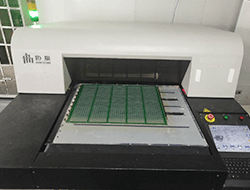
9. Screen Printing
Screen printing is performed on the surface of the flexible circuit board to accurately print text, components and company logos on the board.
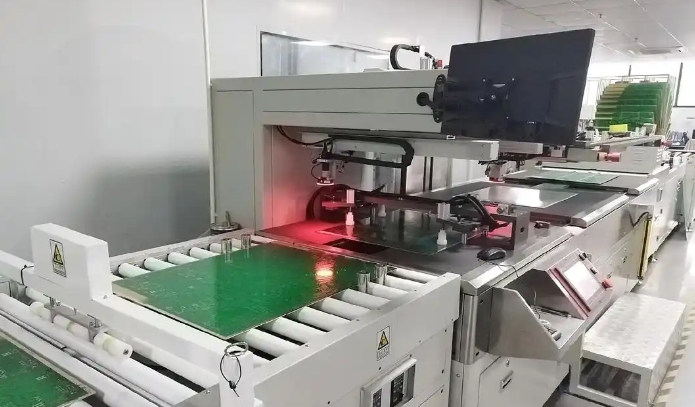
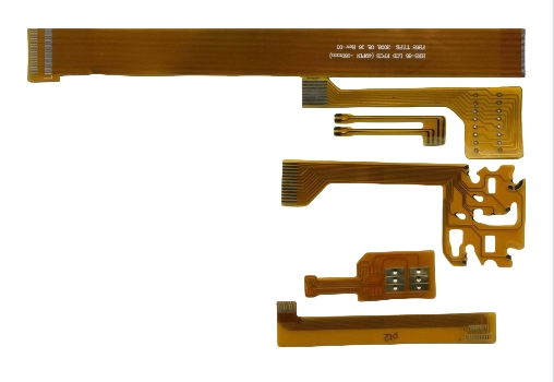
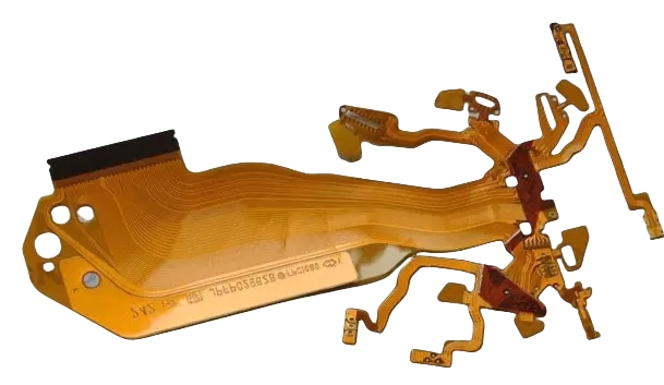
10. Contour Cutting
Cut the circuit board into the final shape according to the design drawing.
10.1 Die Cutting:
Batch cutting using a mold is suitable for large-scale production.
10.2 Blanking Knife:
Cutting using precision tools is suitable for small-batch production capacity requirements.
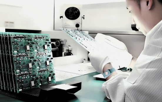
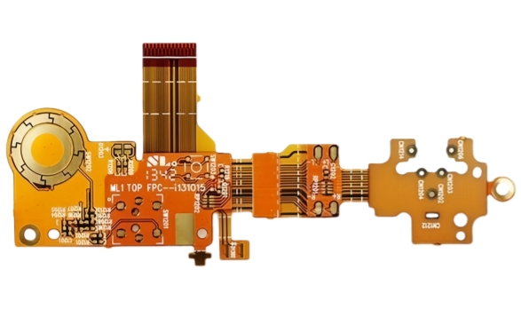
11. Inspection and Testing
Perform comprehensive electrical testing and appearance inspection on the completed flexible circuit board, including conduction test, impedance detection, and bending performance test to ensure that the product meets customer requirements.
| Consumer Electronics | Smartphones, TVs, tablets, and wearables |
| Communication Devices | Smartphones, laptops, tablets, and routers |
| High-Performance Computing (HPC) | Supercomputers, data centers, and cloud servers |
| Medical Equipment | MRI machines, ultrasound devices, and pacemakers |
| Automotive Electronics | Infotainment systems, ADAS, and electric control units |
| Aerospace and Defense | Radar systems, navigation systems, and drones |
| Energy and Power | Solar panels, wind turbines, and energy storage systems |
| Military Electronics | Surveillance systems, communication gear, and weapon systems |
| LED Lighting | LED bulbs, panels, and street lighting |
| Parameter | Description | Unit |
|---|---|---|
| Substrate Material | Polyimide (PI) or Polyester (PET), providing flexibility and thermal stability. | – |
| Copper Foil Thickness | Affects conductivity, typically ranges from 17μm to 70μm. | Micrometers (μm) |
| Trace Width & Spacing | Ensures signal quality and reduces interference. | Millimeters (mm) |
| Total Thickness | Includes substrate, copper layer, and protection film, typically 0.1mm to 0.5mm. | Millimeters (mm) |
| Bending Radius | Minimum is 5 to 10 times the board thickness, affecting flexibility and mechanical performance. | Millimeters (mm) |
| Temperature Range | Maximum operating temperature, typically -40°C to +180°C. | Celsius (°C) |
| Dielectric Constant (Dk) | Electrical characteristic of the material, around 3.2 for polyimide. | – |
| Impedance Control | Characteristic impedance of signal lines, typically 50Ω or 100Ω. | Ohms (Ω) |
| Insulation Resistance | Reflects the insulation performance of the board, higher values indicate better reliability. | Megaohms (MΩ) |
| Thermal Conductivity | Affects heat dissipation in high-frequency and high-power applications. | W/m·K |
| Tensile Strength | The tensile strength of the material, polyimide usually has higher strength. | MPa |
| Surface Treatment | Affects soldering performance; common treatments include gold plating, silver plating, and tin plating. | – |
| Soldering Temperature | Maximum soldering temperature usually 260°C. | Celsius (°C) |
| Fatigue Resistance | Number of bends the board can withstand, suitable for dynamic environments. | – |
| Technical Parameter | Flexible PCB (FPC) | Rigid PCB |
|---|---|---|
| Substrate Material | Polyimide (PI) or Polyester (PET), flexible and heat-resistant. | FR4, rigid material, suitable for static applications. |
| Copper Foil Thickness | 17μm – 70μm, affects electrical performance and flexibility design. | 35μm – 105μm, supports higher current loads. |
| Trace Width & Spacing | Narrow designs due to flexibility limits. | Wider designs for high current/low frequency applications. |
| Total Thickness | Generally 0.1mm to 0.5mm, thin and soft. | Thicker, common thickness of 1.6mm, 2.0mm, etc. |
| Bending Radius | Minimum of 5-10 times the thickness, good flexibility. | Fixed shape, no bending. |
| Temperature Resistance | Max operating temperature up to 180°C. | Typically 100-130°C, lower tolerance. |
| Dielectric Constant (Dk) | About 3.2, affects performance. | Approximately 4.5 for FR4, affects high-frequency performance. |
| Impedance Control | High precision, suitable for high-speed signal transmission. | Suitable for medium to low frequency, less precision. |
| Insulation Resistance | High insulation, suitable for high-frequency applications. | Lower insulation, suitable for general use. |
| Thermal Conductivity | Lower, may require enhanced materials. | Higher, suitable for cooling needs. |
| Surface Treatment | Gold plating, tin plating, etc., improve soldering. | ENIG, HASL, etc., to provide good solderability. |
| Soldering Temperature | Up to 260°C, accommodates high-temperature soldering. | Typically around 260°C, strict control. |
| Fatigue Resistance | Suitable for dynamic bending applications, good fatigue resistance. | Static applications, no fatigue issues. |
| Process | Flexible PCB (FPC) | Rigid PCB |
|---|---|---|
| Material Selection | Polyimide (PI) or Polyester (PET), flexible and heat-resistant. | FR4 or other rigid materials, suitable for static applications. |
| Copper Foil Treatment | Rolled or electroplated copper foil, surface treatment improves performance and adhesion. | Generally simpler treatment, usually rolled or electroplated copper. |
| Etching | Precision etching for high-density circuit creation. | Simple etching methods with larger trace spacing. |
| Photoresist & Development | High-precision exposure and development using photoresist. | Similar process, but larger sizes and no need for bending. |
| Lamination & Curing | Hot-press technology for multi-layer PCB synthesis, maintains flexibility. | Lamination and curing for rigid PCBs, focuses on rigidity. |
| Drilling | High precision, using laser or mechanical drilling techniques. | Precision drilling usually for thicker materials. |
| Surface Treatment & Metallization | Chemical plating, gold/solder plating to enhance solderability and corrosion resistance. | Mainly HASL, gold, and silver plating for stable performance. |
| Screen Printing | Fine process for board identification and patterns, suitable for high-density circuits. | Used for identification and patterns on larger boards. |
HXPCB not only provides flexible PCB production, but also provides flexible PCB assembly services, including designing, manufacturing and assembling flexible circuit boards for various applications. This includes providing solutions for the entire process from material selection to final assembly, ensuring that PCBs meet the specific needs of industries such as consumer electronics, automobiles and medical devices. We are always waiting for your quotation. Our product prices and service quality are better than those of the same industry. HXPCB is your only choice.
The main advantages include lightweight, space-saving, good thermal performance, high reliability, and adaptability to complex designs.
They are widely used in consumer electronics, communication devices, automotive electronics, medical devices, and aerospace industries.
In some cases, the material and manufacturing costs of Flexible PCBs can be higher, but they can offer greater design flexibility and functional benefits in specific applications.
Yes, Flexible PCBs can achieve good soldering quality, especially after metallization, using high-temperature soldering processes.
Flexible PCBs use flexible materials allowing bending, while Rigid PCBs typically use rigid materials suitable for static applications.
The bending endurance typically depends on the material and design, with many flexible PCBs capable of withstanding tens of thousands of bends.
Material selection should consider application environment, operating temperature, electrical performance, cost, and mechanical properties.
Flexible PCBs typically range from 0.1mm to 0.8mm in thickness, varying according to specific application needs.