multi-layer PCB
High-end design,
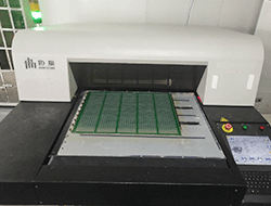
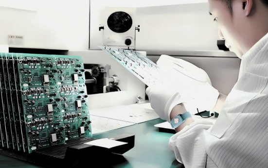
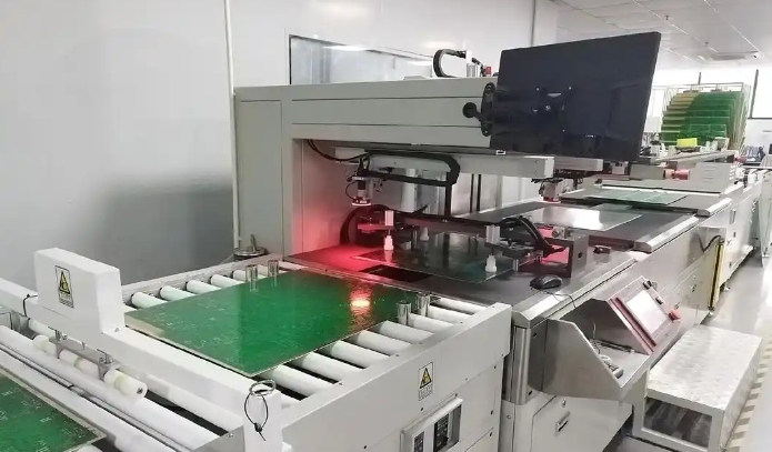
Read MoreHXPCB is a supplier engaged in the PCB industry, providing one-stop production and assembly services such as ordinary PCB, double-sided PCB, multi-layer PCB, aluminum substrate, rigid-flex PCB, HDI PCB, high-frequency PCB and other PCB products. It has strong production equipment and technical team to provide customers with high-quality products, more favorable prices and more considerate services.
交换机.jpg)

.jpg)
.jpg)

poe交换机.jpg)
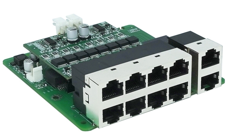
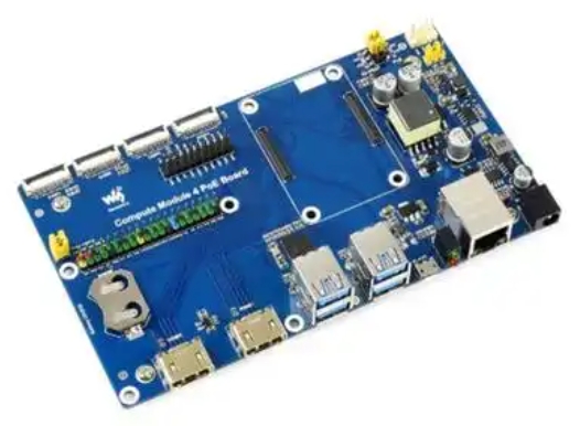
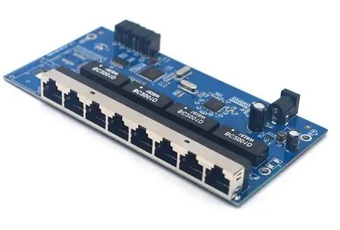
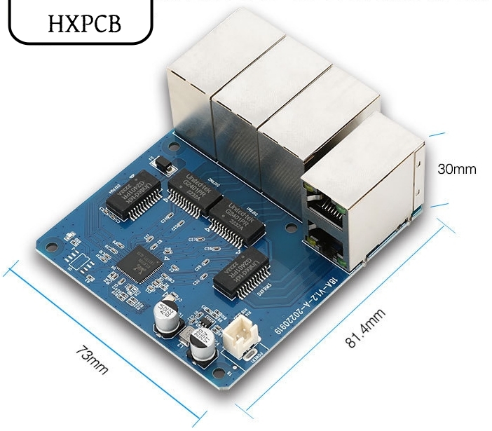
Ethernet Switch PCB is the core printed circuit board (PCB) used in Ethernet switches. It carries all the electronic components and signal routing of the switch and is responsible for receiving, processing, switching and forwarding data packets.

The PCB of high-end Ethernet switches is usually a multi-layer board, with 8~20 layers or even more, to support complex signal routing and power distribution.
High-precision interconnection technology
Ethernet switches usually have multiple ports, and a large number of high-speed signal and power lines need to be arranged on the PCB, requiring high-density interconnect (HDI) design.
Rapid signal transmission
Network data transmission at Gigabit, 10 Gigabit and higher rates (such as 25G, 40G, 100G and above) needs to be met, and the routing needs to be designed as a high-frequency transmission line (such as microstrip line, stripline).
Use low-loss substrates (such as Rogers, PTFE, etc.) to reduce signal attenuation and reflection.
Anti-interference design
In order to reduce signal interference (such as crosstalk and EMI), PCBs need to be shielded, grounded and reasonably laid out.
Heat dissipation treatment
The heat dissipation performance of the PCB is improved by increasing the copper thickness, thermal vias and heat sink design to ensure long-term stable operation of the switch.
Built-in switch chip (Switch ASIC), controller, memory and other core components, perform data packet storage, forwarding and management functions.
Support multi-port high-speed data transmission, forward data packets from the input port to the correct output port.
Requires high-precision routing to ensure signal integrity and low crosstalk.
Supports the connection of electrical ports (RJ45 interface) and optical ports (SFP/QSFP and other optical modules) to ensure high-speed network communication.
Power distribution and management
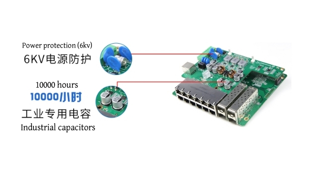
The power management circuit designed by HXPCB provides stable power distribution to power each module of the switch.
Fast heat dissipation performance
Because the switch runs at high load for a long time, the design of the PCB needs to consider the heat dissipation problem. HXPCB increases the copper thickness of the Ethernet switch PCB and increases the heat dissipation channel during production and assembly.
Common materials: FR4 (mid-to-low-end), Rogers, PTFE (Teflon) and other high-frequency materials.
Conductor material: copper foil. High-speed signals usually use thinner copper foil to reduce signal loss.
Applications:
Data center switches, enterprise-level switches, industrial switches, communication base station switches, core router switching equipment
Component procurement and management
Support the assembly of materials (BOM list) provided by customers, provide personalized PCB assembly solutions according to the customer’s switch design requirements to meet special application scenarios, etc., and provide component procurement, verification and supply chain management to ensure high-quality switching chips, interface modules, power modules, etc. meet customer needs.
High-frequency PCB process support
For gigabit high-speed network switches, low-loss substrates (such as Rogers, PTFE) and precision assembly processes are used to ensure high-speed signal transmission performance, and high-speed automated patch equipment is used to accurately mount surface mount components (such as switching chips, capacitors, resistors) on PCBs.
Ensure that precision high-speed signal components (such as ASIC chips, SFP/QSFP interfaces) are stable and reliable.
BGA and micro-component welding
For BGA (ball grid array) packaged chips on high-end switch PCBs, X-ray detection is used to ensure welding quality. Functional testing (FCT), automatic optical inspection (AOI), etc. are provided to ensure that the assembled PCB meets the design requirements.
Whole-machine assembly and integration
The assembled switch PCB is assembled with the chassis, cooling system, power module, etc., and hardware debugging and firmware loading services are provided to deliver finished switches that can be put into use directly.
