Detailed Explanation of the PCB Cloning Process (PCB Circuit Board Cloning)
The technical implementation process of PCB cloning can be briefly described as follows: First, scan the circuit board to be cloned and record the detailed positions of the components. Then, remove the components to create a Bill of Materials (BOM) and arrange for material procurement. The empty board is scanned into an image, which is processed by cloning software to restore it into a PCB file. This PCB file is then sent to a PCB manufacturer for board production. After the board is made, the procured components are soldered onto the PCB. Finally, the board undergoes testing and debugging.
I. Specific Steps of PCB Cloning
- Documenting Components: When you receive a PCB, first record the model, parameters, and positions of all components on paper, especially the orientation of diodes, transistors, and the notch direction of ICs. It’s best to take a few photos of the component positions with a digital camera. Modern PCBs are becoming more advanced, and some diodes and transistors can be easily overlooked.
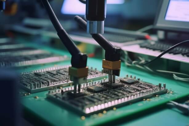
- Removing Components and Cleaning: Remove all components and clean the solder from the PAD holes. Clean the PCB with alcohol and then place it in a scanner. Adjust the scanner to a higher resolution to obtain a clear image. Lightly sand the top and bottom layers with fine sandpaper until the copper layer shines, then scan them again. Use Photoshop to scan both layers in color. Ensure the PCB is placed straight in the scanner; otherwise, the scanned image will be unusable.
- Image Adjustment: Adjust the contrast and brightness of the canvas to create a strong distinction between the copper and non-copper areas. Convert the image to black and white and check if the lines are clear. If not, repeat the adjustment. If clear, save the image as a black and white BMP file (TOP.BMP and BOT.BMP). Use Photoshop to repair and correct any issues.
- Converting to PROTEL Format: Convert the two BMP files into PROTEL format. Load both layers in PROTEL. If the PAD and VIA positions align well, the previous steps were successful. If there are deviations, repeat step 3. PCB cloning requires patience as even minor issues can affect quality and matching.
- Drawing the Layers: Convert the TOP layer BMP to TOP.PCB, ensuring it’s on the SILK layer (yellow). Then, trace the lines on the TOP layer and place components according to the documentation from step 2. Delete the SILK layer after drawing. Repeat this process for all layers.
- Merging Layers: In PROTEL, combine TOP.PCB and BOT.PCB into a single image.
- Verification: Print the TOP LAYER and BOTTOM LAYER on transparent film using a laser printer (1:1 scale). Place the film on the PCB to check for any discrepancies. If everything matches, the cloning is successful.
A cloned board is now complete, but only half the job is done. Testing is required to ensure the electronic performance matches the original board. If it does, the process is truly complete.
Note: For multi-layer boards, carefully sand down to the inner layers and repeat steps 3 to 5. The naming of the images will differ based on the layer count. Cloning multi-layer boards is more complex and prone to alignment issues, so extra care is needed (internal vias and non-conductive holes are particularly problematic).
II. Double-Sided Board Cloning Method
- Scan the top and bottom layers of the PCB and save them as two BMP images.
- Open the cloning software Quickpcb2005, load one of the scanned images, and trace the pads and lines. Save the file as a B2P file.
- Load the other scanned image.
- Open the previously saved B2P file. The traced board will overlay the new image. Disable the top layer lines and silk screen, leaving only the vias.
- Trace the bottom layer lines and save the file. The B2P file now contains both top and bottom layer data.
- Export the file as a PCB file, which can be modified, used to generate a schematic, or sent to a PCB manufacturer.
III. Multi-Layer Board Cloning Method
Cloning a four-layer board is essentially cloning two double-sided boards, and a six-layer board is cloning three double-sided boards. The challenge with multi-layer boards is the inability to see the internal traces. To reveal the inner layers, sanding is the most common and economical method.
After cloning the top and bottom layers, use sandpaper to sand down the surface and reveal the inner layers. Sand evenly and patiently. Silk screen and solder mask will come off quickly, but copper traces will take more effort. Sanding is straightforward but requires patience and effort.
PCB Layout Review
After completing the system layout, review the PCB to ensure optimal results. Consider the following:
- Routing Feasibility: Ensure the layout allows for optimal and reliable routing, and that the circuit will function reliably. Plan the signal paths and power/ground networks during layout.
- Board Dimensions: Verify that the PCB dimensions match the manufacturing requirements and include any necessary markers.
- Component Conflicts: Check for conflicts in 2D and 3D space, especially component heights. For surface-mount components, the height should generally not exceed 3mm.
- Component Arrangement: Ensure components are evenly and neatly arranged. Consider signal types and protection requirements, as well as overall density.
- Component Accessibility: Ensure frequently replaced components are easily accessible and that plug-in boards can be easily inserted into the device.
This detailed process ensures a successful PCB cloning, maintaining the integrity and functionality of the original design.