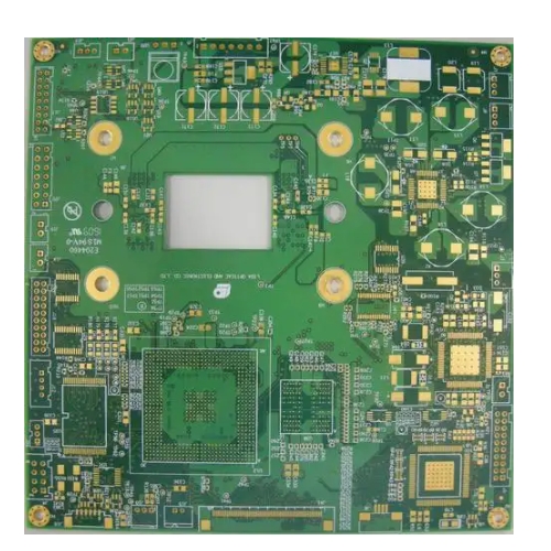
multi-layer PCB
High-end design,
Read MoreHXPCB is a supplier in the PCB industry with more than ten years of experience. We provide copper PCB and various types of PCB manufacturing and assembly services. Our one-stop production and assembly services can save you a lot of time to do efficient things. We have strong production equipment and technical team to provide customers with high-quality products, more favorable prices and more thoughtful services.
Copper PCB refers to a printed circuit board (PCB) that uses copper as the conductive material. Compared with the copper layer coated on the traditional substrate (such as FR-4), copper PCB usually has a thicker copper layer, which enables it to conduct current and dissipate heat better in some special application scenarios. Copper PCB is very common in electronic devices with high power, high frequency or good heat dissipation.
HXPCB is a professional printed circuit board (PCB) manufacturing and assembly service provider with more than 10 years of experience. The company focuses on the research and development and production of high-quality PCB products, and is committed to providing customers with a full range of electronic manufacturing solutions, from single-sided, multi-layer to special material PCB design, manufacturing and finished product assembly, serving customers in the global electronics industry.
1. Excellent thermal conductivity
The thermal conductivity of copper is as high as 401 W/m·K, far exceeding materials such as aluminum (about 237 W/m·K) and FR4 (about 0.3 W/m·K). Copper PCBs can quickly transfer the heat generated by electronics to the heat sink device or the external environment to prevent overheating and significantly improve the life of the equipment.
2. Heat resistance
Copper PCBs can withstand operating temperatures up to 250℃ or even higher, and are not easily affected by high-temperature environments. They are particularly suitable for high-power LEDs, power modules, automotive electronics and other equipment that have strict requirements for heat resistance.
3. Excellent conductivity
Copper has a low resistivity (1.68 × 10^-8 Ω·m), which is more suitable for transmitting high current and high-frequency signals than traditional materials. Copper PCBs have stable conductivity and are suitable for circuit designs that require high frequency, low loss and low impedance.
4. High mechanical strength
Copper materials have extremely high mechanical strength and rigidity, can withstand greater mechanical stress, and are suitable for vibration, shock and life working environments.
Copper-clad PCB refers to a printed circuit board with copper foil as the conductive layer, which is widely used in various electronic devices. heavy copper PCB is its variant, with thicker copper foil (generally ≥35μm), which is suitable for scenarios that require large current or good heat dissipation performance. At the same time, copper-clad PCB refers to a PCB with copper foil on the surface of the PCB, which further improves the conductivity and anti-interference ability of the circuit. Whether it is ordinary copper PCB, thick copper PCB or copper-clad PCB, copper foil is the core material, each with its own characteristics, providing flexible solutions for different electronic applications.
Substrate preparation
1. Select substrate: determine the type of copper substrate to be used.
Substrate cutting: cut the metal substrate into appropriate sizes according to design requirements.
2. Surface treatment
Remove the surface oxide layer: remove the surface oxide layer of the metal substrate by chemical or mechanical methods.
Copper deposition: deposit a thin layer of copper on the metal substrate to facilitate subsequent electroplating and pattern transfer.
3. Photolithography
Coating photosensitive resin: coat a layer of photosensitive material (photoresist) on the surface of the substrate.
Exposure and development: expose the designed circuit pattern to the photosensitive resin through a photomask, and then remove the unexposed photosensitive resin through development, leaving the circuit pattern.

4. Electroplating
Electroplating copper: electroplating is performed on the circuit pattern to form the required copper conductor thickness.
5. Etching
Chemical etching: immerse the substrate in an etching solution to remove excess copper and retain the circuit pattern.

6. Remove photoresist
Cleaning: remove the photoresist with solvents or chemicals to expose clear copper conductors.
7. Drilling and Metallization
Drilling: Drill holes on the PCB according to the design requirements.
Hole Metallization: Electroplate a thin layer of copper in the hole to ensure electrical connection between different layers.
High-power LED fixtures, LED streetlights, LED automotive headlights
5G base station RF modules, microwave communication devices, filters, power amplifiers
Inverters, industrial controllers, sensors, drive circuit modules
High-power components in smartphones, tablets, and smart wearable devices
Switch-mode power supplies, power regulators, industrial power supplies
New energy vehicle battery management systems (BMS), onboard LED lighting systems, motor control systems, automotive radar modules
| Application Area | Application Scenarios |
| High-Power LED Lighting | High-power LED fixtures, LED streetlights, LED automotive headlights |
| Power Modules and Power Management Systems | Switch-mode power supplies, power regulators, industrial power supplies |
| Automotive Electronics | New energy vehicle battery management systems (BMS), onboard LED lighting systems, motor control systems, automotive radar modules |
| Communication Equipment and RF Modules | 5G base station RF modules, microwave communication devices, filters, power amplifiers |
| Industrial Automation Equipment | Inverters, industrial controllers, sensors, drive circuit modules |
| Military and Aerospace Fields | Radar systems, satellite communication modules, missile guidance systems |
| Consumer Electronics | High-power components in smartphones, tablets, and smart wearable devices |
| Parameter | Description |
| Substrate Material | Aluminum base, copper base, or other metal substrates |
| Copper Thickness | Typically 1oz-6oz, or more |
| Total Thickness | Based on design requirements, commonly 1.6mm, 2.0mm, or thicker |
| Minimum Trace Width | Usually 0.1mm or smaller, depending on manufacturing process and design requirements |
| Minimum Spacing | Typically 0.1mm or smaller, depending on design and manufacturing capabilities |
| Thermal Conductivity | Thermal conductivity of copper is about 400 W/m·K, and aluminum is about 205 W/m·K |
| Insulation Material | Typically epoxy resin, polyimide, or other low-dielectric materials |
| Dielectric Constant | Generally around 3.5, depending on insulation material |
| Thickness Tolerance | Usually ±10% or ±15%, depending on manufacturing standards |
| Surface Treatment | Hard gold, lead-free tin plating, immersion gold, OSP, etc. |
| Temperature Range | Typical operating temperature is -40°C to +125°C; special designs can withstand higher temperatures |
| Dielectric Strength Test | Depending on design requirements, typically 1500V or 3000V |
HXPCB’s PCB assembly service includes one-stop services for design, manufacturing, parts procurement, production, and testing, which efficiently ensures that customers can obtain reliable solutions and save time and cost. HXPCB assembly (PCBA) service is committed to meeting customer configuration needs, covering all stages from prototype design to mass production.
Copper-based PCBs have excellent thermal and electrical conductivity, allowing for effective heat dissipation and making them suitable for high-power electronic devices.
They are widely used in LED lighting, power modules, automotive electronics, communication devices, etc.
Major steps include design, substrate preparation, surface treatment, photolithography, electroplating, etching, hole metallization, and insulation coating.
Copper PCBs can typically operate safely in high-temperature environments, with a common operating temperature range from -40°C to +125°C.
Consider working temperature, dielectric constant, and thermal performance; epoxy or polyimide is typically used as insulation material.
Copper thickness directly impacts current-carrying capacity, thermal performance, and mechanical strength; thicker copper layers can carry larger currents and provide better heat dissipation.
Applying protective coatings such as OSP or immersion gold can help prevent oxidation and improve corrosion resistance.
Generally, the minimum trace width and spacing are around 0.1mm, but it varies depending on design requirements and manufacturing capabilities.
Common surface treatments include lead-free hot air leveling, immersion gold, and OSP (organic solderability preservative); the choice depends on usage requirements and costs.
Copper-based PCBs may have a higher cost compared to traditional PCBs, but their performance and reliability provide significant advantages in many applications.