multi-layer PCB
High-end design,
Read More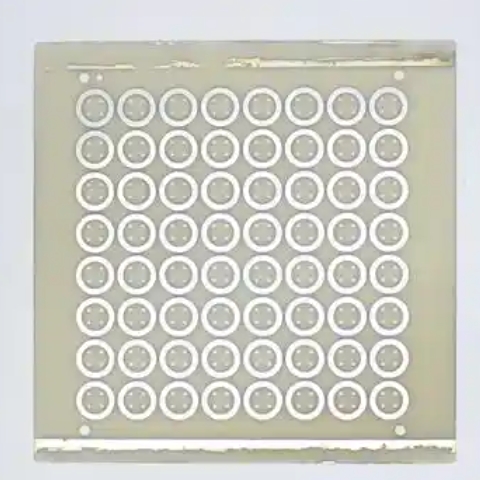
.jpg)


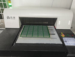
Substrate preparation
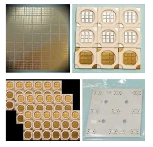
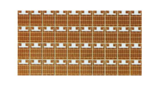
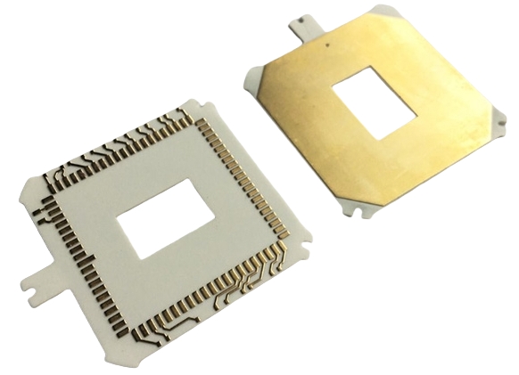
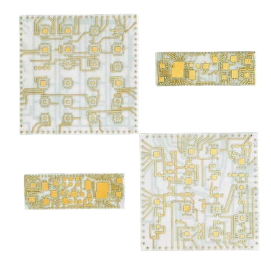
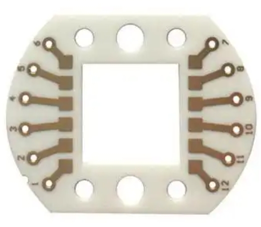
The substrate of ceramic PCB usually adopts ceramic materials such as aluminum oxide (Al2O3), aluminum nitride (AlN), silicon nitride (SiN). The preliminary process includes cutting the ceramic material into the required size and shape.

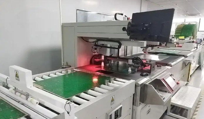
Circuit pattern transfer
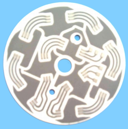
A layer of photoresist is applied to the surface of the ceramic substrate, and then the circuit pattern is transferred to the photoresist by ultraviolet light irradiation. Then it is developed to leave the graphics of the circuit pattern, and then according to the design requirements, holes are punched on the ceramic substrate to form the necessary electrical connection channels.
Electrode deposition
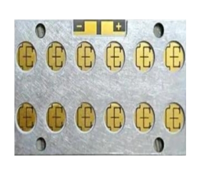
Conductive metals (such as gold, silver, copper, etc.) are deposited on the surface of the ceramic substrate through evaporation, sputtering or chemical vapor deposition (CVD) and then the metal layer is thickened by electroplating to ensure the conductivity of the circuit.

Sintering process
After the metal deposition is completed on the ceramic substrate, sintering treatment is required to ensure good bonding between the metal and the ceramic substrate.
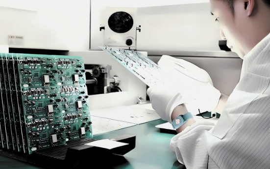
Surface treatment
After the circuit pattern and metal deposition are completed, the ceramic PCB is surface treated, such as tin plating, gold plating, etc., to improve weldability and reliability.