BGA PCB Assembly Services
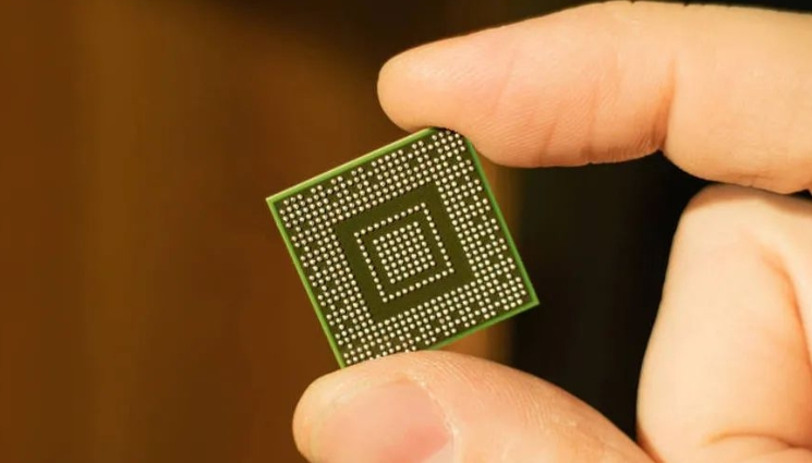
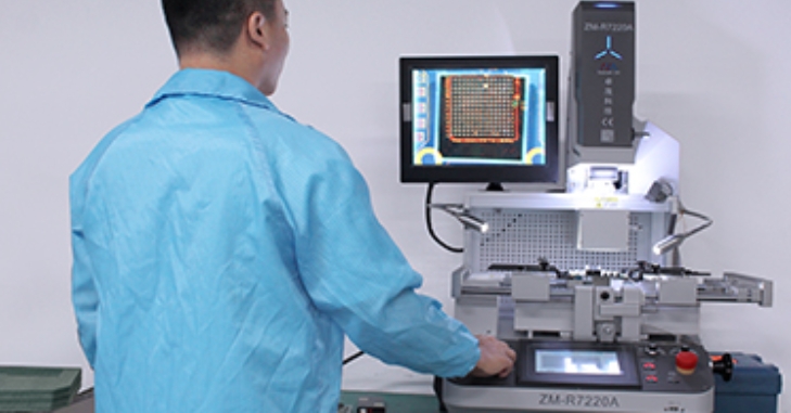
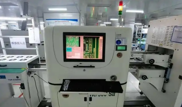
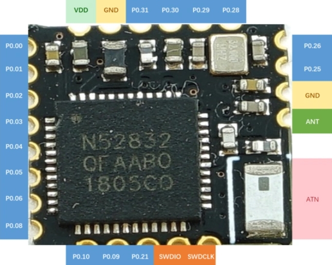
Selected PCB samples BGA PCB assembly display
HXPCB focuses on the research and development of ultra-large size circuits board, multi-layer PCBs, metal-based PCBs, rigid-flex high-frequency PCBs, HDI PCBs, and related processes. We offer comprehensive services, including PCB design, prototyping, processing, and assembly.


What is BGA PCB Assembly and How Does It Work?
BGA PCB assembly (Ball Grid Array PCB Assembly) refers to the process of assembling a printed circuit board (PCB) for surface mount components using a ball grid array (BGA) package. BGA is a surface mount package where the component is connected to the PCB via solder balls arranged in a grid pattern underneath the component (rather than the more traditional pins).
Here is how BGA PCB assembly works:
1.BGA package design: BGA components have small solder balls arranged in a grid pattern on the bottom of the component, allowing these solder balls to serve as electrical and mechanical connections between the component and the PCB.

2.Placement on PCB: BGA components are placed on the PCB using an automatic pick and place machine, followed by reflow soldering (the solder balls are aligned with the pads on the PCB to which they will be soldered).
3.Inspection: Since BGA solder joints are located underneath the component, they are not visible after assembly. Advanced inspection techniques such as X-ray inspection are used to inspect the quality of the solder joints and ensure proper assembly.
4. Testing: Electrical and functional testing of the assembled PCB is performed to ensure that the BGA components and the overall PCB are functioning properly.
BGA PCB assembly process
The BGA PCB assembly process usually includes the following steps:
Apply solder paste: Apply a layer of solder paste evenly on the pad of the PCB. This step is the key to subsequent soldering. The solder paste is usually applied by stencil printing technology or spraying technology to ensure the uniform application of the solder paste.
Place solder balls on pads: Use automated equipment (such as a placement machine) to accurately place the solder balls of the BGA chip on the PCB pads that have been soldered with solder paste. Subsequently, the solder balls of the BGA chip come into contact with the solder paste.
Reflow soldering: After the PCB and BGA components are placed, the entire PCB will enter the reflow soldering furnace for heating. By heating the solder paste to the melting point, the BGA solder balls and the PCB pads form an initialized solder connection.
Cooling and curing: After the reflow soldering is cooled, the PCB will slowly cool in the cooling area to solidify the solder joints.

Inspection and testing: After the matching is completed, automatic inspection (AOI), X-ray detection and other technologies are used to check the BGA soldering quality to ensure that there are no problems such as cold soldering, leaking soldering, open circuits or short circuits.
Difficulties in BGA PCB assembly process
1.Soldering quality problems
1. Inaccurate BGA solder ball alignment may cause poor welding or even circuit breakage.
2. BGA solder balls may have poor welding conditions such as cold welding, virtual welding or bridging, which will affect signal transmission and electrical performance.
Countermeasures:
1. Use a high-precision alignment system SMT machine to ensure that the BGA and PCB pads are correctly docked.

2. Ensure that the BGA solder balls are completely melted at the appropriate temperature by accurately controlling the reflow soldering temperature curve to avoid overheating or underheating.
3. Use X-Ray equipment to detect the internal quality of the solder joints and confirm whether there are virtual solder joints, virtual solder joints or bridging phenomena in the welding.
2.Solder ball alignment error problem
1. BGA components may have a slight offset when placed, causing the solder balls to be misaligned with the PCB pads, making welding difficult and prone to solder joint disconnection or electrical instability.
2. When the solder balls are misaligned, short circuit bridging is easily formed, especially when there are more pins in the BGA package, the problem is more prominent.

Countermeasures:
1. Use a high-resolution visual positioning system to check the alignment of BGA solder balls and PCB pads to ensure the accurate position of each solder ball.
2. Use automatic optical inspection (AOI) or X-Ray to re-confirm the BGA welding quality and detect potential problems in time.
3.Solder joint porosity problem
1. During the welding process, gas may be trapped in the solder joint, resulting in the formation of pores and affecting welding reliability.
2. Since pores are usually located inside the solder joint, conventional detection methods cannot detect pores.
Countermeasures:
1. Ensure the stability of the welding environment atmosphere, reduce the influence of oxidation, humidity and other factors, and avoid the generation of pores during welding.
2. Choose low-gassing solder to reduce the generation of pores during welding.
3. Use X-Ray technology to image the inside of the solder joint to detect and correct the pore problem in time.
Disadvantages of BGA PCB Assembly
High Soldering Difficulty
BGA packages have high pin density, small ball diameter, and are arranged at the bottom, which makes the soldering process complicated.
Soldering requires highly sophisticated equipment and processes, and ordinary SMT (surface mount technology) equipment may not meet the requirements.
Poor reliability and maintainability
Once the BGA chip is soldered to the PCB, it is almost impossible to directly observe or test the soldering quality of its pins, making subsequent repairs difficult.
If a BGA chip fails, the entire chip usually needs to be replaced, and the repair cost is high.
For equipment that needs maintenance or upgrades, BGA packaging may pose greater challenges.
Advantages of HXPCB for BGA PCB assembly
Efficient Space Utilization
Our BGA technology allows us to select the optimal pcb layout, thus optimizing the PCB design of compact devices. Making it ideal for applications where space is critical.
Better Heat Dissipation and Conductivity
Our BGA provides excellent heat dissipation and conductivity, reducing thermal stress and signal loss.
Higher Manufacturing Efficiency
Advanced assembly processes combined with sophisticated equipment ensure higher yields, reduce rework and improve overall manufacturing efficiency.
Reduced Wire Stress
The robust design of the BGA package minimizes mechanical stress on PCB traces and wires during operation, thereby increasing the durability and life of the component.
Reduced Costs
Our BGA assembly process reduces labor costs, and our technical support and staffing can reduce assembly time, reducing the operating and maintenance expenses of the final product.
Quality Assurance
HXPCB implements strict quality control measures, including X-ray and AOI inspections, to ensure defect-free assembly.
HXPCB's BGA PCB assembly capabilities
| Category | Details |
|---|---|
| Supported BGA Types | Plastic BGA (PBGA), Ceramic BGA (CBGA), Ultra-Thin BGA (UTBGA), Chip-On-Package (CoP), Stacked Die BGA (SDBGA), Wafer-Level BGA (WLBGA), Fine-Pitch BGA (FPBGA), Quad Flat No-Lead (QFN) Packages |
| Assembly Size Range | Minimum: 3mm x 3mm / 2mm x 2mm; Maximum: 40mm x 40mm / 45mm x 45mm |
| Pitch Tolerance | Minimum pitch size: 0.35mm; Placement accuracy: +/- 0.025mm |
| Layer Support | Capable of assembling PCBs with up to 40 layers |
| Passive Component Sizes | Compatible with 01005, 0201, 0402, 0505, Press-fit components, Package-on-Package (POP) |
| Advanced Equipment | High-speed pick-and-place machines, precision solder jet printers, multi-zone reflow ovens, inline X-ray systems, and high-definition AOI systems |
| Service Types | Embedded Die BGA, High-Density BGA, Multi-Chip Module (MCM) Assembly, Organic Substrate BGA (OSBGA), and Hybrid Material BGA Assembly |
| Testing Capabilities | Functional testing, Boundary-scan testing, Real-time X-ray imaging, BGA Rework and Repair services, AOI and Solder Paste Inspection (SPI) |
Industries That Benefit from BGA Assembly
Automotive Electronics: For safety systems, infotainment, and power control units.
Telecommunications: High-performance communication devices, routers, and network equipment.
Consumer Electronics: Smartphones, wearable devices, and other high-performance consumer goods.
Medical Devices: Critical medical equipment requiring highly reliable components.
FAQ
Frequently Asked Question
Compared with traditional packaging (such as DIP and QFP), BGA designs the pins (solder joints) as solder balls, which are located at the bottom of the chip. This makes the pin density of BGA packaging higher, suitable for high-performance, compact electronic devices, and has better electrical performance and thermal management capabilities.
Since the solder joints of BGA are located inside the package and cannot be directly observed by the naked eye, the following detection methods are usually used:
X-Ray detection: X-rays can be used to penetrate the BGA package to check the internal quality of the solder joints and avoid problems such as cold solder joints and cold solder joints.
Automatic optical inspection (AOI): Check the soldering quality on the outside after soldering and check whether the solder balls have bridging, misalignment and other problems.
Electrical testing: Conduct in-circuit testing (ICT) and functional testing to ensure normal electrical connections.
The alignment of BGA components usually uses high-precision placement machines and automatic visual alignment systems (AOI). These systems can accurately align BGA with PCB pads to ensure accurate solder ball position and avoid soldering problems.
The temperature control of reflow soldering in BGA assembly is very important, and a multi-temperature zone reflow soldering oven is usually used to ensure uniform temperature distribution. The reflow soldering oven is usually equipped with three temperature zones: preheating, reflow and cooling to ensure that the BGA solder balls are completely melted and avoid thermal damage.
The solder balls of BGA are located at the bottom of the chip and are not visible after welding. Traditional visual inspection cannot directly confirm the welding quality. Therefore, BGA welding requires the help of X-Ray equipment for internal inspection. In addition, because BGA solder joints are small and dense, reflow soldering temperature control and alignment accuracy are required to be higher.
Since the thermal expansion coefficient of BGA components is different from that of the PCB substrate, the soldering process may cause PCB warping. To prevent warping, it is recommended to:
Use a PCB substrate with good thermal stability.
During the reflow soldering process, use a suitable fixture or support device.
Optimize the soldering temperature curve to ensure uniform heating.
The difference between the thermal expansion characteristics of BGA package and PCB substrate may cause solder joint fatigue in thermal cycle. To improve the thermal cycle stability, it is recommended to:
Consider the thermal expansion coefficient of BGA in the PCB design stage and select the appropriate substrate material.
Use lead-free solder to increase the thermal fatigue resistance of solder joints.
Perform thermal cycle test to verify the reliability of BGA welding under different temperature environments.
Cold solder joints: refers to the solder joint surface that looks like it has been soldered, but the internal electrical connection is not fully formed, usually caused by insufficient temperature or too much solder.
Cold solder joints: due to insufficient temperature, the solder is not completely melted, and the solder joint surface presents a poor connection state, which usually leads to poor electrical contact.
Avoidance methods:
Optimize the reflow soldering temperature curve to ensure that the solder is fully melted.
Use reliable quality solder.
Use X-Ray for internal solder joint inspection.