Ultimate Guide to PCB Manufacturing Process: From Design to Final Product
The Printed Circuit Board (PCB) manufacturing process is a complex sequence of steps that transforms a conceptual design into a functional electronic product. This guide delves into the technical intricacies of PCB manufacturing, covering everything from design to the final product. We will explore the physical principles behind each step, data-driven insights, and real-world applications to provide a comprehensive understanding of the process.
Introduction to PCB Manufacturing
A Printed Circuit Board (PCB) is a board made of insulating material, such as fiberglass or plastic, with conductive pathways etched onto its surface. These pathways connect different electronic components, enabling the functioning of modern electronic devices. The PCB manufacturing process involves multiple stages, from design to assembly, each requiring precision and technical expertise.
Key Terms Explained
- Substrate: The base material of the PCB (e.g., FR4, a common fiberglass-reinforced epoxy laminate).
- Conductive Traces: The copper pathways that connect components on the PCB.
- Soldering: The process of joining components to the PCB using a fusible metal alloy.
Design and Prototyping
The PCB design process begins with creating a schematic diagram of the circuit using specialized software like KiCad or Altium Designer. The schematic is then translated into a physical layout, considering factors such as trace width, spacing, and thermal management.
Design Considerations
- Signal Integrity: Ensuring minimal signal loss and interference.
- Power Distribution: Designing robust power and ground planes.
- Thermal Management: Managing heat dissipation to prevent component failure.
Prototyping Tools
- Gerber Files: Standard files used to communicate PCB designs to manufacturers.
- Bill of Materials (BOM): A list of components required for assembly.
Materials Selection
The choice of materials significantly impacts the performance, durability, and cost of a PCB. Common materials include:
| Material | Properties | Applications |
|---|---|---|
| FR4 (FR-4) | Cost-effective, rigid, and suitable for most consumer electronics. | Consumer electronics, IoT devices. |
| High-Tg FR4 | Higher thermal stability for demanding applications. | Automotive and industrial electronics. |
| Rogers (PTFE) | Low loss, high-frequency applications. | RF and microwave circuits. |
Fabrication Process
The fabrication process involves creating the physical PCB from the design files. Key steps include:
1. Photolithography
- Process: A photoresist material is applied to the copper-clad substrate. Ultraviolet light is used to expose the resist through a photomask, creating a pattern of conductive traces.
- Physics Behind It: The photoresist material undergoes a chemical change when exposed to UV light, allowing it to be developed and etched.
2. Etching
- Process: The exposed copper is removed using a chemical etchant, leaving behind the desired conductive pathways.
- Chemical Reaction: Ferric chloride or ammonium persulfate is commonly used to etch copper.
3. Drilling
- Process: Holes for through-hole components or vias are drilled using CNC machines.
- Precision: Drill bits are typically 0.1mm to 6.0mm in diameter.
4. Plating
- Process: A thin layer of copper is plated onto the walls of drilled holes to create conductive vias.
- Surface Finish: Options include HASL (Hot Air Solder Leveling), ENIG (Electroless Nickel Immersion Gold), and OSP (Organic Solderability Preservative).
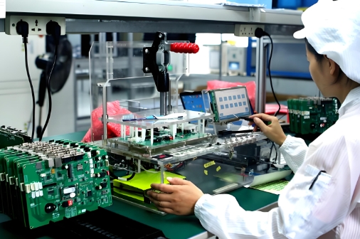
Assembly and Testing
Once the PCB is fabricated, the next step is to assemble the components and test the board.
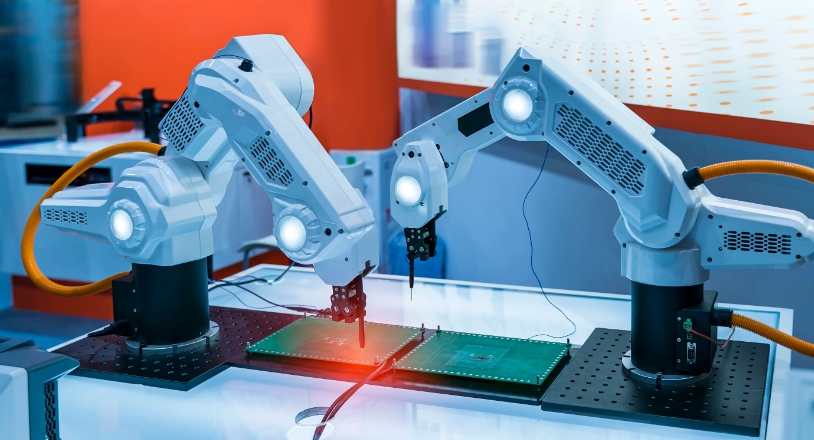
Surface Mount Technology (SMT)
- Process: Components are mounted onto the PCB using automated pick-and-place machines.
- Soldering: A reflow oven melts the solder paste, securing the components to the board.
Testing
- Functional Testing: Verifying that the PCB operates as intended.
- In-Circuit Testing (ICT): Checking for shorts, opens, and component values using probes.
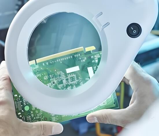
Quality Control and Inspection
Ensuring the quality of a PCB involves multiple inspection steps:
1. Optical Inspection (AOI)
- Process: Automated systems scan the PCB for defects such as soldering issues or component misalignment.
- Data Visualization: Defects are highlighted in real-time for quick resolution.
2. X-Ray Inspection
- Process: Used to inspect hidden solder joints, especially in high-density PCBs.
Applications and Industry Use Cases
PCBs are ubiquitous in modern electronics. Some notable applications include:
- Consumer Electronics: Smartphones, laptops, and tablets.
- Automotive Systems: Engine control units, infotainment systems, and ADAS (Advanced Driver-Assistance Systems).
- Medical Devices: MRI machines, pacemakers, and portable defibrillators.
- Aerospace: High-reliability PCBs for satellites and aircraft systems.
FAQs and Troubleshooting
Q: What is the minimum trace width for a PCB?
A: The minimum trace width depends on the current and voltage. For low-current applications, traces can be as narrow as 0.1mm.
Q: How do I prevent soldering defects?
A: Ensure proper solder paste application, precise component placement, and controlled reflow oven parameters.
Conclusion
The PCB manufacturing process is a blend of art and science, requiring meticulous attention to detail and a deep understanding of materials and physics. By following this guide, engineers and manufacturers can optimize their workflows, reduce defects, and produce high-quality PCBs for a wide range of applications.
Further Reading
For a deeper dive into PCB manufacturing, explore these resources:
