In the rapidly evolving electronics industry, PCB manufacturing and assembly form the backbone of modern hardware innovation. From consumer gadgets to industrial machinery, the quality of printed circuit boards (PCBs) directly impacts product performance, durability, and compliance. This guide dives deep into advanced techniques, industry standards, and emerging trends in PCB production, offering actionable insights for engineers, procurement specialists, and OEMs seeking reliable partners for their projects.
(1).The PCB Manufacturing Process: From Design to Delivery
1.Design for Manufacturability (DFM): The Foundation of Success
A flawless PCB begins with meticulous design. Engineers must adhere to DFM guidelines to avoid costly revisions. Key considerations include:
Trace Width/Spacing: Ensuring compliance with IPC-2221 standards to prevent short circuits or signal interference.
Layer Stackup: Optimizing signal integrity and thermal management for high-speed or high-power applications.
Material Selection: Choosing substrates like FR-4, Rogers, or polyimide for thermal stability and dielectric performance.
Pro Tip: Use simulation tools (e.g., Ansys SIwave) to validate EMI/EMC performance before prototyping.
2.Advanced Fabrication Techniques
Modern PCB fabrication involves precision-driven processes:
Laser Direct Imaging (LDI): Replaces traditional photomasks for micron-level accuracy in trace patterning.
Controlled Depth Drilling: Critical for HDI (High-Density Interconnect) boards with microvias (<100µm).
Plasma Etching: Ensures clean via walls for reliable plating in multilayer designs.
Case Study: A medical device manufacturer reduced signal loss by 30% using 18-layer rigid-flex PCBs with blind/buried vias.
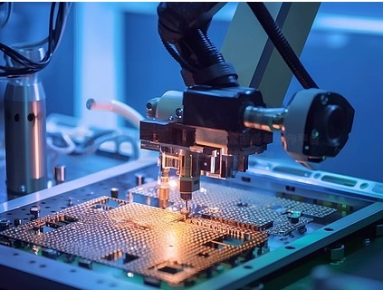
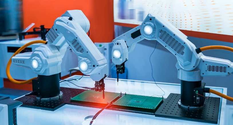
3.Surface Mount Technology (SMT) Assembly: Speed and Precision
SMT assembly dominates modern PCB production, offering advantages like:
Automated Pick-and-Place Systems: Achieve placement accuracy of ±25µm for 01005 components.
Reflow Soldering Profiles: Customizable thermal curves for lead-free SAC305 or low-temperature BiSnAg alloys.
3D SPI (Solder Paste Inspection): Prevents defects like insufficient solder or bridging with real-time feedback.
Industry Insight: Automotive-grade PCBs require AEC-Q100-qualified components and -40°C to 150°C thermal cycling tests.
(2).Quality Assurance: Meeting Global Standards
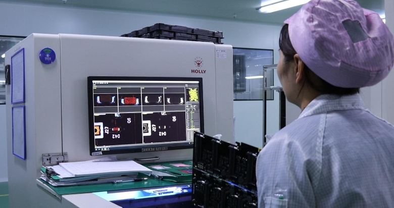
1.In-Process Testing and Inspection
Automated Optical Inspection (AOI): Detects missing components or misalignments with 99.98% accuracy.
X-Ray Inspection: Verifies BGA solder joint integrity and via fill quality.
In-Circuit Testing (ICT): Validates electrical functionality against design specifications.
2.Compliance and Certifications
IPC-A-600/610: Defines acceptability criteria for PCB workmanship.
ISO 9001 & IATF 16949: Ensures traceability for automotive and aerospace applications.
RoHS/REACH: Mandatory for EU markets to restrict hazardous substances.
Data Point: Boards compliant with UL 94 V-0 flame-retardant standards reduce safety risks in power electronics.
Emerging Trends in PCB Technology
1.Rigid-Flex PCBs: Enabling Compact Designs
Combining rigid and flexible sections, rigid-flex PCBs are ideal for wearables and IoT devices. Benefits include:
40% weight reduction compared to traditional interconnects.
Improved shock/vibration resistance in automotive applications.
2.Embedded Components and Advanced Packaging
Die Embedding: Integrates bare dies into substrate layers for RF/microwave systems.
Fan-Out Wafer-Level Packaging (FOWLP): Supports 5G/mmWave frequencies with minimal signal loss.
3.Sustainability in PCB Manufacturing
Halogen-Free Laminates: Meet eco-label requirements (e.g., Blue Angel).
Water Recycling Systems: Reduce wastewater in copper plating processes by up to 90%.
Choosing a PCB Manufacturing Partner: Key Considerations
When outsourcing PCB manufacturing and assembly, prioritize partners who:
Offer ITAR-registered facilities for defense projects.
Provide 24/7 production monitoring via IoT-enabled systems.
Support NPI (New Product Introduction) with rapid prototyping (<72-hour turnaround).
(3).Conclusion: Precision, Compliance, and Innovation
he future of PCB manufacturing and assembly lies in mastering advanced technologies while adhering to rigorous quality standards. By partnering with a certified manufacturer that invests in cutting-edge equipment (e.g., 6-axis laser drills, AI-driven AOI) and maintains transparent communication, businesses can accelerate time-to-market and achieve long-term reliability in their electronic products.
Whether you’re developing a prototype or scaling to mass production, understanding these technical nuances ensures your PCBs meet the demands of tomorrow’s innovations—from AI-driven edge devices to electric vehicle powertrains.The above sharing comes from HXPCB. If you have other insights, please leave a message for discussion.
