multi-layer PCB
High-end design,
Read MoreHXPCB focuses on the research and development of ultra-large size circuits board, multi-layer PCBs, metal-based PCBs, rigid-flex high-frequency PCBs, HDI PCBs, and related processes. We offer comprehensive services, including PCB design, prototyping, processing, and assembly.
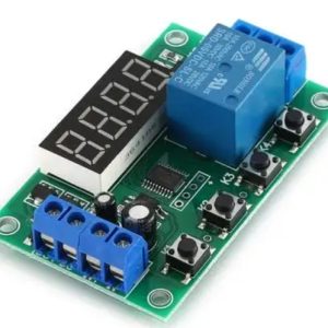
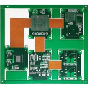
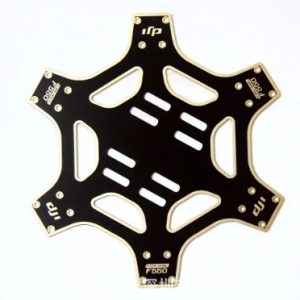
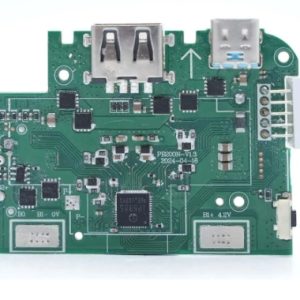
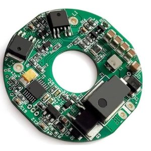

We offer both manual and automated insertion services for through-hole (TH) components. Axial-leaded components have leads extending from both ends of the component, while radial-leaded components have both leads extending from the same side.

We provide PCB encapsulation services to effectively protect electronic components from physical impact and chemical attack. This solution is ideal for environments that require long-term stable operation and helps improve the performance and reliability of electronic devices.
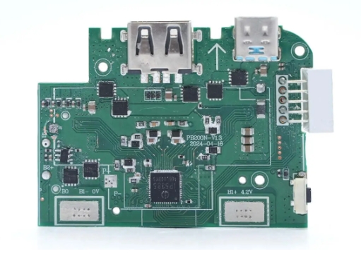
We use automated through-hole assembly processes to precisely mount radial and axial components. This method can significantly reduce the error rate, speed up the production cycle, while reducing material operations and labor expenses, and has extremely high economic benefits.

In through-hole PCB assembly, we offer a variety of conformal coating solutions to protect electronic components from environmental factors, impurities, and aggressive chemicals. These coatings include materials such as acrylic, parylene, polyurethane, epoxy, and silicone.
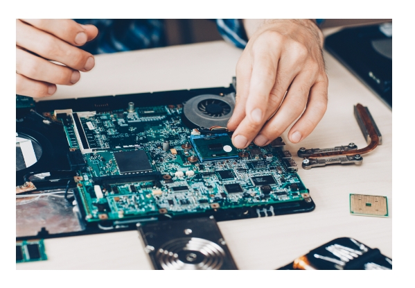
The technology is suitable for small batch production and also supports the installation of customized components and sub-assemblies on circuit boards. Manual assembly can also be used to supplement automated processes, especially when component positions that are difficult for automatic inspection equipment to identify require manual verification and necessary corrections.

Manual soldering stations are used to mount through-hole components onto circuit boards. This method is usually suitable for low-volume production or prototyping. Manual soldering for through-hole PCB assembly usually takes longer than other processes.
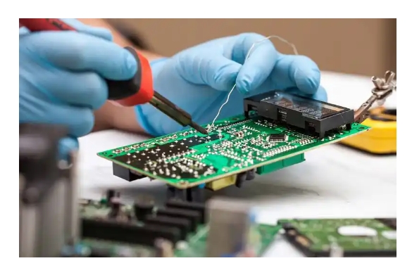
It uses a solder bath to help solder individual through-hole components on PCBs. It is faster, more repeatable, and produces more reliable results than manual soldering.

Wave soldering is faster and provides higher joint reliability than manual soldering, making it an ideal process for high-volume through-hole PCB assembly.
Through-Hole PCB Assembly is a traditional electronic assembly technology in which electronic components are inserted into pre-drilled PCB through-holes (Through-Hole) through pins and fixed to the back or other layers of the PCB by soldering. The reliability and mechanical strength of this technology are widely evaluated in electronic devices that require high reliability or increased mechanical vibration.
1. Component Installation
Manual Insertion: Manually insert components into through-holes, suitable for assembly of small batches or complex circuits.
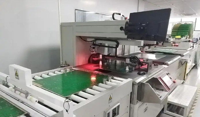
Automatic Insertion: Use an automatic insertion machine (such as a pin insertion machine) to insert components into pre-drilled through-holes, suitable for mass production.
2. Wave Soldering
The PCB is fed into the wave soldering furnace, and the wave component pins are soldered to the PCB through the molten solder to ensure fast mechanical and electrical connections.
3. Manual Re-soldering
For parts or special components that are difficult to handle with automatic soldering, manual soldering is used for re-soldering or repair. This is usually used for small batch production or prototype production.
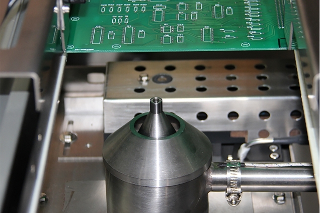
4. Inspection and Repair
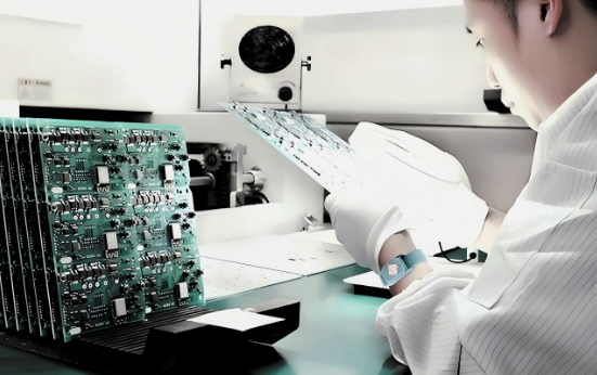
Optical inspection equipment (AOI) is used to check the welding quality to ensure that each solder joint meets the requirements. Manual inspection can repair bad solder joints or misplaced components.
5. Functional Test
Electrical performance and functional tests are carried out to ensure that the PCB after through-hole assembly meets the design requirements and all circuit connections are normal.
6. Cleaning
Clean the PCB to eliminate residues during the welding process to avoid affecting the long-term use of the circuit.
| Feature | Description |
|---|---|
| 1. Reliable Component Insertion and Welding Technology | Use of advanced technology for consistent and durable connections. |
| 2. Rigorous Assembly Plan | Detailed planning process to ensure quality and efficiency during assembly. |
| 3. Combination of Wave Soldering and Manual Soldering | Utilizing both methods for optimal soldering results, catering to various component needs. |
| 4. Customized Service and Design Support | Tailored solutions and assistance in design to meet specific customer requirements. |
| 5. Product Quality Control | Strict quality control measures to maintain high standards throughout the production process. |
| 6. Fast Delivery and Efficient Production | Streamlined processes to ensure timely delivery without compromising quality. |
| 7. Compliance with International Standard Testing | Adherence to international testing standards to guarantee product reliability and safety. |
Through-hole PCB assembly provides higher mechanical strength and durability, is suitable for high-power, high-current applications, and is convenient for later maintenance.
Through-hole PCB assembly usually requires materials such as PCB board, components, solder, soldering tools and cleaners. The choice of materials depends on the design requirements of the circuit board.
The lead time depends on the size and complexity of the order. Typically, small-volume orders have shorter lead times, while large-volume orders take longer.
We ensure the assembly quality meets the standards through a strict quality control process including automatic optical inspection (AOI), X-ray inspection and functional testing.
Through-hole technology solders components by inserting component pins into holes, while surface mount technology (SMT) solders components directly to the PCB surface. Through-hole is suitable for applications that require stronger physical connections, while SMT is more suitable for high-density, high-speed assembly.
Yes, many PCBs can use both through-hole and surface mount technology, called hybrid assembly. This allows the advantages of both technologies to be used to meet different design needs.
Yes, we provide customized through-hole PCB assembly services, designing and optimizing the assembly process according to the specific needs of customers.
The cost of through-hole PCB assembly depends on several factors, including the number of PCB boards, component types, assembly complexity, and production batch.
