DFMA (Design for Manufacturability and Assembly) is the abbreviation of “Design for Manufacturing and Assembly”. It is a design methodology that aims to ensure that products can be easily and efficiently produced and assembled during the design stage. The goal of DFMA service is to optimize product design, reduce production costs, improve manufacturing efficiency, and ensure the feasibility and reliability of products during the production process.
Why is DFMA service needed?
Avoid mistakes made by design companies Reduce communication costs and disputes Reduce product development iterations Reduce time to market Provide proactive suggestions to customers to save costs and shorten production time Reduce defects in PCB manufacturing and assembly and improve yields Save product launch costs Improve equipment reliability and service life
Required Materials
There are many types and brands of materials required for PCB, so we cannot prepare all materials in advance, but we will strictly abide by the customer’s wishes, and we may suggest suitable substitutes to the customer. If the customer cannot accept it, we can also purchase the specified type/brand according to the customer’s design.
Free service
We evaluate the manufacturability of your product design and analyze issues in your design that may affect production processes and quality. We provide free design optimization advice to our customers. We help customers simplify their designs and reduce unnecessary parts. Provide free preliminary cost estimates. Provide free prototyping and production process advice. Check the design files provided by customers and provide feedback on manufacturability and assembly. Provide free design specification and standard consultation services to help customers understand industry best practices, quality standards and manufacturing requirements.
CAM Design
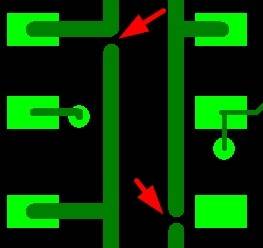
Copper traces
Disconnection
The etched characters are reverse characters, for example, the bottom layer is positive and the top layer is negative. In some cases, the front and back sides of the etching are also a basis for judging the wiring level.
The distance from the pad to the edge of the board is too small, which can easily cause damage to the pad during contour processing.
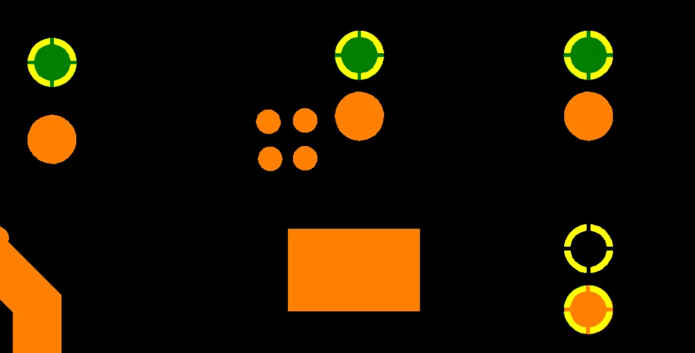
The thermal pad overlaps the isolation pad and continuity cannot be determined.
The isolation area between the power supply and the ground is too small, and the connecting wires are in the same network.
The distance between circuits is too small.
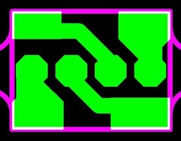
The distance between the inner spacers is too small.
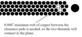
Dummy copper pads should be added to large non-copper areas to prevent bending or twisting.
Drilling in separate areas
Solder Mask
Forgot to put fiducial marks on the solder mask.
The solder mask opening on the fiducial is too large.
There are additional solder mask openings on the pads/traces.
Edge connectors are not completely free of solder mask.
Silkscreen
If silkscreen errors are significant, they can cause problems for our PCB assembly process. Additionally, unclear, incomplete, or crowded silkscreens are not aesthetically pleasing. Therefore, our CAM engineers also check and ask if there are any errors. Common errors include: silkscreen over pads, crowded, beyond the edge of the board, too small, overlapping, has negative text on it, etc.
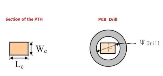
drill
Vias overlay PTH holes. Hole attributes in drawing are NPTH, but there is pad/ring around drill hole.
Special holes are not marked. Special holes can sometimes be imported by EDA software, so they must be marked on the drill drawing.
The drilling size is the same as the pin size of the PTH component.
Blind and buried vias
Blind and buried vias are designed to reduce the size of the PCB and improve its functionality. Although we can produce any layer with HDI PCB, we always recommend using a symmetrical structure as it is easier to produce and reduces the chances of bending and twisting.
What we offer for free DFA
PCB manufacturability testing
Before production, we will do a thorough DFM on the PCB, mainly including the following document checks.
Materials
Stacking
PCB Panel
Hole: PTH, NPTH,
Processing Hole, Mounting Hole
Benchmark
Solder Point Clearance
Component clearance
Copper connection
Solder mask color
Silk screen
UL logo/PCB supplier
PCB panel
Surface treatment recommendations
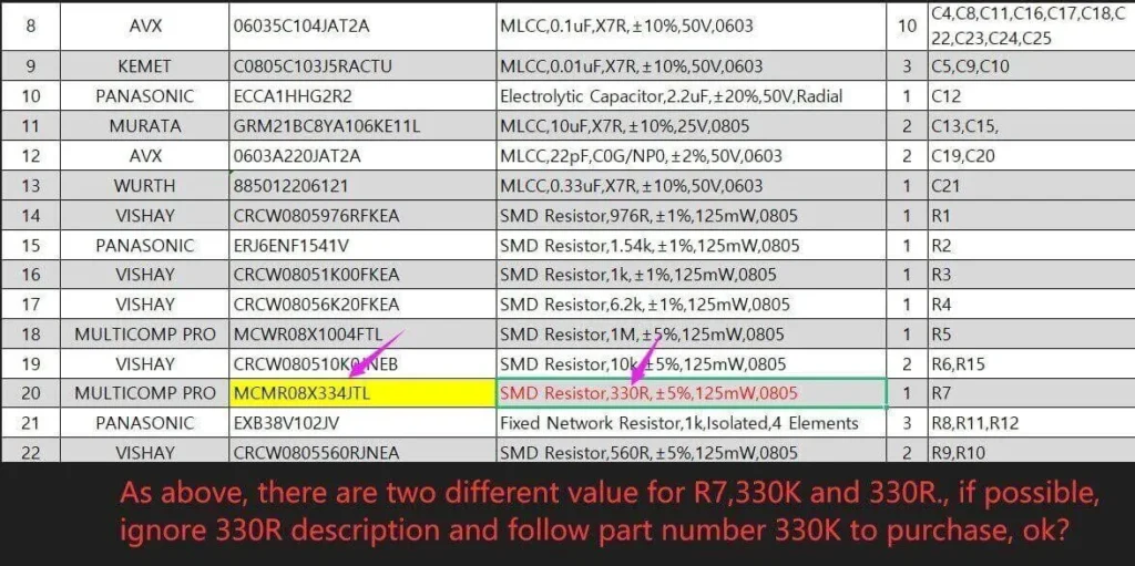
BOM Check
The important functions of PCBA are as follows.
The parts on the BOM do not match the pads or drill holes on the PCB.
Where component part numbers are unclear or incomplete, we will inquire with the customer and suggest the correct part number where possible.
Alternative suggestions
Sometimes some parts are obsolete or have long lead times, we will suggest alternatives whenever possible and only use them in production after customer approval.