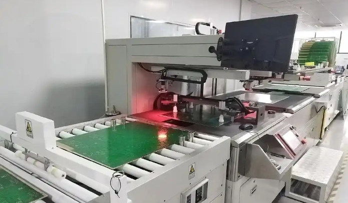
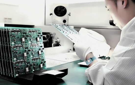
PCB Manufacturing and Assembly
Printed circuit
Read MoreHXPCB is a supplier engaged in the PCB industry. We provide one-stop production and assembly services for ordinary PCB, double-sided PCB, multi-layer PCB, aluminum PCB, rigid-flex PCB, HDI PCB, drone PCB and high-frequency PCB. Our production equipment and technical team enable us to have more favorable prices for our high-quality products.
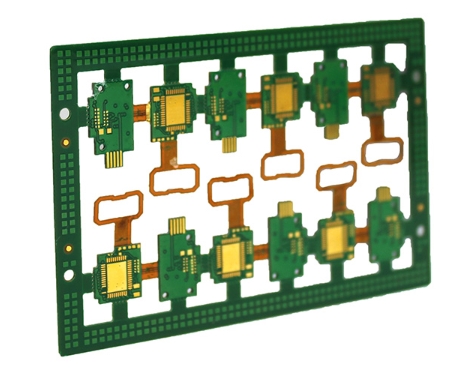

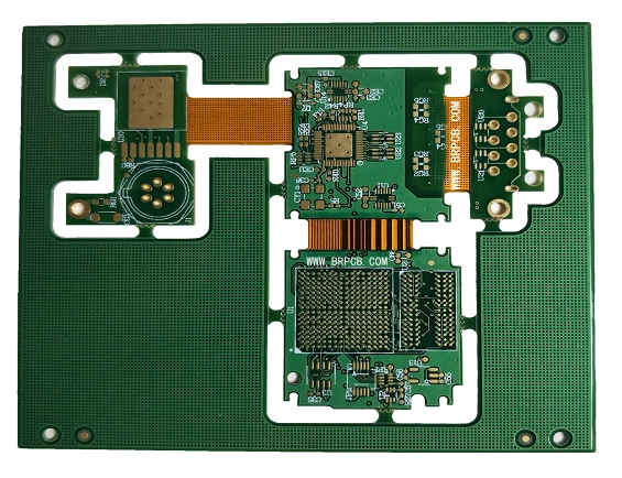
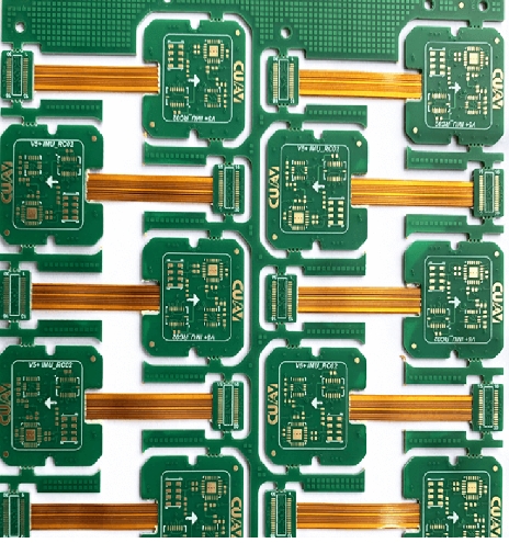

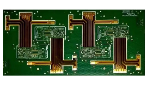

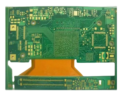

HXPCB provides customers with high-quality rigid-flex PCB and manufacturing assembly services. Our rigid-flex solutions combine the mechanical strength of rigid boards with the flexibility of flexible circuits to achieve compact, lightweight and reliable designs to meet the various needs of modern industries.
With more than ten years of experience, HXPCB is committed to providing customized rigid-flex PCB solutions for multiple fields such as consumer electronics, automotive, aerospace and medical equipment. Choosing HXPCB, you will benefit from our commitment to quality, innovation and customer service. Whether it is prototyping or mass production, we can optimize your design to improve efficiency and durability.
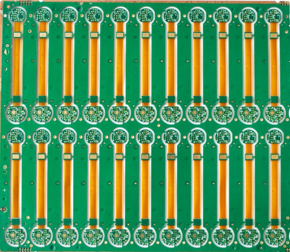
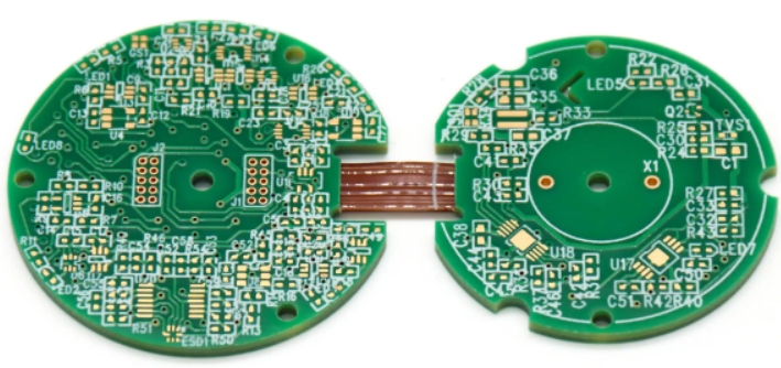
Rigid-Flex PCB is a circuit board structure that combines the advantages of flexible circuit board (FPC) and rigid circuit board (Rigid PCB). It integrates flexible materials and rigid materials together to achieve a perfect combination of the mechanical strength of rigid circuit board and the foldability and bendability of flexible circuit board. It can provide stability in fixed areas and allow free bending of movable parts in one design.
Features
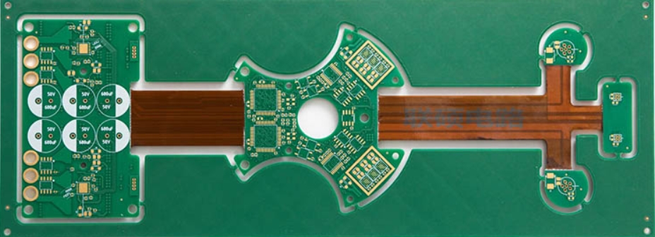
1.Structural features: Rigid-flex boards are composed of multiple layers of flexible and rigid materials. The flexible parts are usually located in areas that need to bend or move, while the rigid parts are used to support components or provide mechanical strength.
2.Functional features: They meet multiple functional requirements in a single design, reducing the need for connectors and cables while optimizing the structure of electronic devices.
3.Manufacturing features: Compared with traditional flexible or rigid PCBs, rigid-flex boards require more complex design and manufacturing processes, especially lamination and drilling accuracy.
Advantages
Reduce connectors and cables, improve the reliability and performance of signal transmission.
1.Save PCB space and enhance the overall design flexibility of the device.
2.Improve system stability by reducing solder joints and connection points.
3.Enhance durability, making it suitable for complex environments and bending requirements.
1.Material Selection and Matching
The rigid sections typically use FR4, while the flexible sections use polyimide. Ensuring the compatibility of these materials in terms of thermal expansion (CTE), adhesive bonding, and mechanical properties is crucial to prevent delamination or warping during manufacturing and usage.
2.Layer Stack-Up Design
Designing an optimal stack-up that meets electrical performance, mechanical strength, and bending requirements is challenging. Engineers must balance the thickness of rigid and flexible layers, manage impedance control, and minimize signal integrity issues.
3.Precise Lamination Process
The lamination of rigid and flexible materials involves strict process controls to avoid misalignment, wrinkles, and voids. The thermal and mechanical stresses during lamination can lead to defects if not handled properly.
4.Drilling and Via Management
The transition between rigid and flexible areas poses challenges for drilling and via plating. Ensuring reliable connections without damaging the delicate flexible materials requires advanced techniques and precise process controls.
5.Reliability Testing
Rigid-Flex PCBs must undergo rigorous bending, thermal cycling, and vibration tests to ensure durability. Simulating real-world conditions and validating long-term reliability are key aspects for engineers.
6.Manufacturing Yield and Cost
The complexity of Rigid-Flex PCBs increases the risk of manufacturing defects, such as open circuits, delamination, or misalignment. These issues not only affect yield but also significantly raise production costs.
1. Rigid material (FR4)
FR4 is the standard material for the rigid part and is widely adopted due to its excellent mechanical strength, thermal stability and cost-effectiveness.
2. Flexible material (polyimide)
Polyimide (PI) is the preferred material for the flexible layer, with high heat resistance, low dielectric constant and excellent flexibility.
3. Adhesive
The adhesive (such as epoxy or acrylic) used to connect the rigid and flexible layers is critical.
Cover film and protective layer
The flexible area is usually covered with a polyimide cover film for insulation and mechanical protection.
4. Copper foil
High-quality copper foil is the basis for signal transmission.
5. Reinforcement material
In a specific design, engineers may add reinforcement materials such as FR4 or stainless steel to the flexible area to increase mechanical support and ensure reliable performance.
| Application Field | Specific Uses | Communication Devices | Mobile phones, tablets, wireless terminals |
| Medical Equipment | Portable medical instruments, monitoring devices, implantable devices |
| Automotive Electronics | In-car navigation, driver assistance systems, power management systems |
| Consumer Electronics | Smart wearables, virtual reality devices, gaming consoles |
| Industrial Control | Automation devices, testing instruments, control panels |
| Aerospace | Avionics, satellite communication devices, navigation systems |
1. Design stage
Design for manufacturability (DFM):
Ensure that the design of the rigid-flexible board can be manufactured by existing processes, including the folding radius of the flexible area, the location of vias, and the thickness of the copper foil.
Material selection:
Select appropriate rigid materials (such as FR4, Rogers) and flexible materials (such as PI polyimide) according to the application.
2. Material preparation
Flexible material processing:
Use flexible substrates (such as polyimide PI) and copper foil to obtain double-sided or single-sided flexible circuit boards through calendering or lamination.
Rigid material processing:
Use FR4 or other rigid substrates to prepare single-sided or multi-layer rigid boards.
3. Circuit etching
Flexible part:
Etch the flexible circuit pattern on the flexible substrate, while considering the bending resistance, usually designed as a curved routing.
Rigid part:
Etch the circuit pattern of the rigid area, and select different multi-layer structures according to the number of layers.
4. Multilayer lamination
Pre-alignment of flexible and rigid layers:
Precisely align the flexible layer and the rigid layer through molds or optical methods.
Multilayer lamination: Use hot pressing and vacuum technology to press rigid materials and flexible materials together to ensure that the flexible area remains pressure-free. Special protective adhesive film or coverlay is required during the lamination process.
Coverlay lamination: Cover the PI film on the flexible area to protect it while maintaining flexibility.
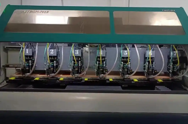
5. Drilling and metallization
Drilling: Use a mechanical drill or laser drill to drill holes in the board (including vias, through holes, etc.).
Hole metallization: Chemical copper plating and electroplating of the drilled holes to form a conductive path.
6. Surface treatment
Perform surface treatment as required, such as OSP, lead/lead-free tin spraying, immersion gold, immersion silver, etc.
7. Shape processing
Use mechanical cutting, CNC processing or laser cutting to shape the rigid part to ensure that the flexible part remains intact.
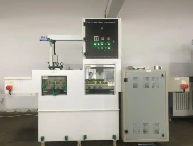
8. Testing and inspection
Electrical testing: Test the conductivity and insulation performance to ensure that there is no open circuit or short circuit.
Bending test: Test the bending performance of the flexible area to verify reliability.
Appearance inspection:
Check the quality of the press fit, the integrity of the hole metallization, and the quality of the cover film.
| Parameter | English | Typical Range/Value |
|---|---|---|
| Materials | Rigid Materials | FR4, Rogers; thickness: 0.2mm–3.2mm |
| Flexible Materials | Polyimide (PI); thickness: 0.05mm–0.2mm | |
| Copper Thickness | Copper Thickness | 1 oz–3 oz (35μm–105μm) |
| Layer Count | Layer Count | 2–12 layers; advanced up to 20 layers |
| Minimum Hole Size | Mechanical Drilling | 0.2mm–0.3mm |
| Laser Drilling | 0.1mm–0.2mm | |
| Minimum Line Width/Spacing | Line Width/Spacing | 50μm–100μm (2mil–4mil) |
| Flex-to-Rigid Transition | Bending Radius | ≥10× the flex thickness |
| Transition Type | Reinforced or smooth transitions | |
| Surface Finish | Surface Finish | ENIG, HASL, OSP, Immersion Silver/Tin |
| Bend Life | Bend Life | Over 10,000 cycles |
| Impedance Control | Impedance Control | Tolerance: ±5% for critical signal layers |
| Temperature Range | Operating Temperature Range | -40°C to 125°C; high-performance up to 150°C |
| Parameter | Rigid-Flex PCB | Standard PCB |
|---|---|---|
| Materials | Combination of rigid (e.g., FR4) and flexible (e.g., PI) materials | Rigid materials only (e.g., FR4, CEM-1, CEM-3) |
| Layer Count | Typically 2–12 layers; advanced designs up to 20 layers | Typically 2–12 layers; advanced designs up to 64 layers |
| Flexibility | Flexible regions allow dynamic or static bending | Entirely rigid, no flexibility |
| Minimum Line Width/Spacing | 50μm–100μm (2mil–4mil), more challenging due to hybrid material processing | 75μm–100μm (3mil–4mil), less complex |
| Minimum Hole Size | 0.1mm (laser drilling), 0.2mm (mechanical drilling) | 0.2mm (mechanical drilling), limited laser drilling use |
| Copper Thickness | 1 oz–3 oz (35μm–105μm), customizable for rigid and flex areas | 1 oz–3 oz (35μm–105μm), uniform across the board |
| Bending Radius | ≥10× the flex thickness, critical for reliability | Not applicable |
| Impedance Control | High precision (±5%) required for high-speed signals due to varied material properties | Easier to control due to homogeneous materials |
| Thermal Management | Complex due to different material properties and flex zones | Relatively simple, homogenous thermal profile |
| Surface Finish | ENIG, OSP, HASL, Immersion Silver/Tin for both rigid and flexible areas | ENIG, HASL, OSP, Immersion Silver/Tin |
| Applications | High-reliability and space-saving designs (e.g., aerospace, medical devices, foldable devices) | General-purpose applications (e.g., consumer electronics, industrial equipment) |
| Manufacturing Cost | Higher due to complex processes and hybrid materials | Lower due to simpler processes and standard materials |
| Assembly Complexity | Requires specialized handling for flex zones | Easier assembly with automated processes |
| Reliability | High, especially in dynamic applications; flex regions must endure mechanical stress | High for static and rigid environments |
| Durability | Durable under dynamic conditions (e.g., bending, flexing) | Durable in static conditions, prone to cracks if stressed |
| Parameter | Rigid-Flex PCB | Standard PCB |
|---|---|---|
| Base Material | Combination of rigid (FR4) and flexible (Polyimide, PI) materials | Rigid only (FR4, CEM-1, CEM-3) |
| Dielectric Constant (Dk) | Rigid: 4.2–4.5 (FR4); Flex: 3.2–3.5 (PI) | 4.2–4.5 (homogeneous across the board) |
| Loss Tangent (Df) | Rigid: 0.015–0.025; Flex: 0.002–0.008 (lower for PI) | 0.015–0.025 |
| Thermal Conductivity | Rigid: 0.3–0.5 W/m·K; Flex: 0.1–0.3 W/m·K | 0.3–0.5 W/m·K |
| Glass Transition Temperature (Tg) | Rigid: 130°C–170°C; Flex: 200°C+ for high-performance materials | 130°C–170°C |
| Decomposition Temperature (Td) | Rigid: ~300°C; Flex: ~400°C for Polyimide materials | ~300°C |
| CTE (Coefficient of Thermal Expansion) | Rigid: 12–16 ppm/°C; Flex: ~20 ppm/°C for PI | ~12–16 ppm/°C |
| Moisture Absorption | Rigid: ~0.15%; Flex: ~0.6% (higher for PI) | ~0.15% |
| Tensile Strength | Rigid: ~350 MPa; Flex: 150–200 MPa | ~350 MPa |
| Flexibility | Flexible materials allow dynamic or static bending | Not applicable |
| Material Thickness | Rigid Layers: 0.2mm–3.2mm; Flex Layers: 0.05mm–0.2mm | Uniform: 0.2mm–3.2mm |
| Adhesive Layer | May include adhesive-free copper for improved flexibility | Adhesive is not a concern for rigid materials |
| Surface Finish Compatibility | Suitable for ENIG, HASL, OSP, Immersion Silver/Tin | Suitable for ENIG, HASL, OSP, Immersion Silver/Tin |
HXPCB provides high-quality rigid-flex PCB assembly services designed to meet the advanced needs of industries such as aerospace, medical devices, telecommunications, and consumer electronics. Our rigid-flex solutions combine the flexibility of flexible PCBs with the stability of rigid boards, providing excellent durability, high performance, and space-saving advantages. Whether you need a complex multi-layer design or a precise flex-to-rigid conversion, HXPCB’s experienced team can ensure perfect assembly, providing reliable, high-speed, and lightweight solutions to meet your specific requirements.
Rigid-Flex PCBs combine rigid and flexible materials, making them suitable for applications requiring space-saving and flexible designs. Standard PCBs are entirely rigid, suitable for traditional electronic devices. Rigid-Flex boards can withstand bending, unlike standard PCBs.
Rigid-Flex PCBs are designed to operate under dynamic conditions and can endure bending and flexing, resulting in relatively high durability. In suitable operating environments, their mechanical and electrical performance remains stable, making them suitable for demanding applications.
The minimum hole size for Rigid-Flex PCBs is 0.1mm (laser drilling) to 0.2mm (mechanical drilling). Laser drilling can provide smaller hole sizes but is more expensive, so it’s essential to consider design requirements and budget constraints when choosing a drilling method.
The design of flexible areas must consider bending radius and environmental factors. Typically, flexible materials should be less than 0.2mm thick, and the bending radius should be at least 10 times the material thickness to ensure reliability and durability. Thorough simulations and testing are crucial before design finalization.
Due to design complexity and the presence of flexible areas, the packaging of Rigid-Flex PCBs often requires more specialized techniques to prevent damage and deformation during manufacturing and assembly. Standard PCB packaging is relatively straightforward and often easier to automate.
The electrical performance of Rigid-Flex PCBs is influenced by materials and designs. The use of different materials necessitates precise impedance control to ensure high-frequency signal transmission quality. Appropriate surface finishes and material compositions can further enhance electrical performance.
When selecting materials for Rigid-Flex PCBs, consider application needs, operating environments, and performance specifications. Rigid parts typically use FR4 or other high-frequency materials, while flexible sections can use Polyimide (PI) or other suitable flexible materials to ensure compliance with design requirements and usage conditions.
The manufacturing process of Rigid-Flex PCBs involves design, material selection, substrate fabrication, component assembly, testing, and final quality inspection. Key factors include ensuring a reliable connection between the rigid and flexible parts and maintaining strict quality control at every stage of the process.
The minimum hole size for Rigid-Flex PCBs depends on the drilling method used. For mechanical drilling, the minimum hole size is typically 0.2mm, while laser drilling can achieve smaller hole sizes down to 0.1mm.
The bending radius for flexible sections of a Rigid-Flex PCB is typically 10 times the thickness of the flexible material. For example, a 0.1mm thick flex section should have a minimum bending radius of 1mm.
